TABLE OF CONTENTS
Chapter 1 Introduction ...................................................................................................................2
1.1 The Package Contents ................................................................................................................................2
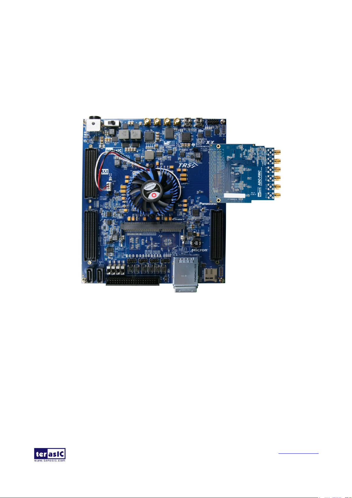
1.2 Assemble ADC-FMC with FPGAMainboard............................................................................................3
1.3 Connectivity ...............................................................................................................................................4
1.4 Getting Help...............................................................................................................................................5
Chapter 2 Architecture of ADC-FMC .............................................................................................. 6
2.1 Features.......................................................................................................................................................6
2.2 Component and Layout ..............................................................................................................................6
2.3 Block Diagram............................................................................................................................................8
Chapter 3 Using the ADC-FMC ...................................................................................................... 9
3.1 Pin Definition of FMC Connector..............................................................................................................9
3.2 Using the ADC Chip AD9648BCPZ-125.................................................................................................13
3.3 Select reference clock source for ADC.....................................................................................................14
Chapter 4 ADC Demonstrations ................................................................................................... 16
4.1 Demo Block Diagram...............................................................................................................................16
4.2 Demo on TR5 FPGA Mainboard..............................................................................................................17
4.3 Demo on Intel A5SoC FPGA Mainboard.................................................................................................19
Chapter 5 Appendix ..................................................................................................................... 22
5.1 Revision History.......................................................................................................................................22
5.2 Copyright Statement.................................................................................................................................22