TK ZX81 Instrucciones de funcionamiento e instalación

06.04.2018 Page 1 of 16
ZX81 - 32KB internal RAM
Build-up description
06.04.2018
Cop right
Histor Histor Histor Histor Histor
V1.0
06.04.2018

06.04.2018 Page 2 of 16
Introduction
The idea behind the ZX81 – 32KB internal RA project goes back into the 1990‘s where Peter Liebert-Adelt created a
32KB internal RA extension to enhance the ZX81 capabilities.
(see ZX81 webpage: http://www.zx81.de/hardware/32k-ramd.htm)
I‘ve taken this idea, because I‘d liked to enhance my own ZX81. So based on above page I build a small PCB board
(without the backup battery buffer) that can be directly placed into your ZX81 after doing some solderwork.
I’d like to say thank you to the following helping hands (ZX Team members), providing support in different flavours:
•S. Engel aka Siggi
•P.Liebert-Adelt aka Peter Liebert-Adelt
•J. erkl aka Joachim
•H. Junek aka ZX-Heinz
06.04.2018 - TOKABLN aka T. Kapke (Berlin – Germany)

06.04.2018 Page 3 of 16
Table of content
1 GENERAL BUILD UP TIPS...................................................................................................4
2 32KB INTERNAL RAM EXTENSION.....................................................................................5
2.1 Short description ..............................................................................................................5
2.2 Component List (default) ..................................................................................................7
2.3 32KB PCB component placement(s) in pictures .................................................................8
3 TIME TO DO SOME TESTING ...........................................................................................15
4 SCHEMATIC....................................................................................................................16

06.04.2018 Page 4 of 16
1General build up tips
As always when soldering electronic components, you should start with the smallest components, e.g. Resistor, Diodes
first following next size components until all components are soldered.
THIS IS TYPICALLY NOT DONE BY THE SUPPLIER OF YOUR PURCHASED PACKAGE.
06.04.2018 Page 5 of 16
232KB internal RAM extension
2.1 Short description
This little PCB board gives you full 32K-RA internal memory from 16K to 32K and from 48K to 64K.
The schematic is shown at the end of this document… while here’s a small description:
IC1 is a 74LS00 circuit (4 NAND gates in a S D SOIC housing), while we only use 2 of the NAND gates as follows:
When the ULA is forced to output the display-file to your screen, this is indicated to the ULA with the signal / 1 =
LOW and A15 = HIGH. Because the display-file is located in the 16-32K area of your ZX81, A15 for the RA must be
LOW when / 1 = LOW. The two NAND-gates take care about this situation. As we are using 2 NANDs this will form an
AND at the end.
Resistor R1 is used optionally if you like to use HRG8 screen mode. I’ll recommend adding this component.
IC2 is a H 62256-70 SRA PDIP housing IC (32Kx8 RA -chip) all these parts enables your ZX81 to have at least 2 x
16KB of RA available. So let’s start to upgrade your ZX81.
First work items to be done is, to open your ZX81 and to carefully remove the PCB board to do some reworks which
allows the usage of the new 32KB internal RA board. Having the ZX81 board carefully detached from the keyboard
flat cables, please start locating the existing RA chip(s).
•Depending on your PCB issue, remove the original 1 or 2k memory chip(s) from your ZX81 PCB. If the memory
chip(s) is/are soldered, I recommend to cut the IC leads on top of the PCB with a side-cutting tool and to
unsolder the remaining leads afterwards.
oThen use a solder sucker or some solderwick to get the remaining solder out of the solder pads
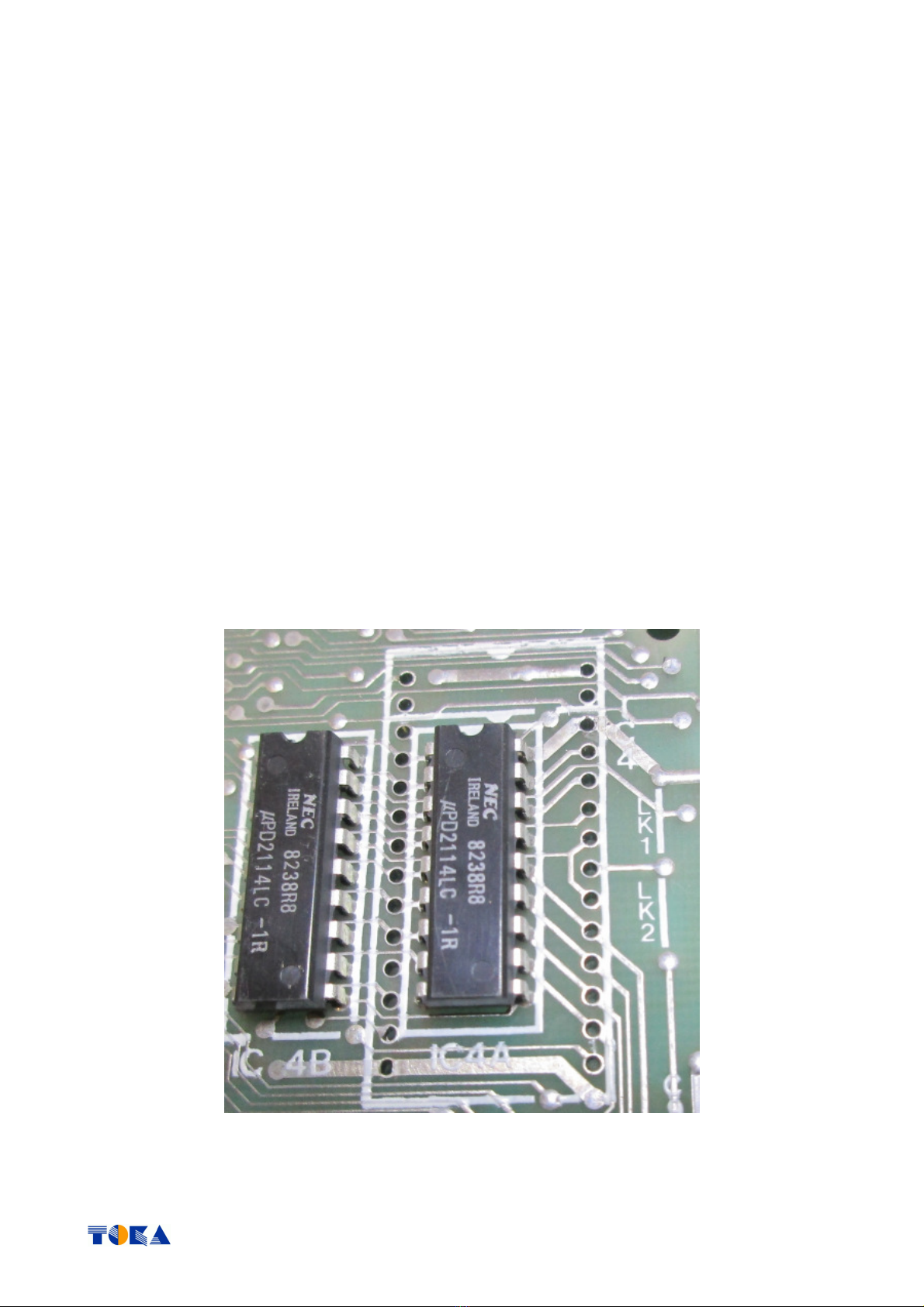
(example picture ZX81 Issue 3 board)

06.04.2018 Page 6 of 16
•After you successfully removed the old RA chips and you’ve cleaned the solder pads, solder a standard IC-
socket with 28 pins at the place of IC4 (take care about the orientation… the notch needs to point to the edge
connector of your ZX81 PCB).
oIf you use precision pin headers instead of the standard pin headers, you may solder a precision IC
socket rather the standard one. But when using the above shown pin headers, only a standard
socket will work.
•Having finished soldering the IC socket, fit some short wire at the place of LK2 (see above LK1/LK2 silk print at
the right side of IC4)
That’s all for the first time when it comes to the ZX81 PCB board.
Now let’s start assembling the new 32KB PCB board.

06.04.2018 Page 7 of 16
2.2 Component List (default)
Resistors:
1x
S D 0805 - 10K ohm resistor (optional for HRG8 usage) R1
ICs:
1x
IC 74LS00 S D SOIC (NAND chip) IC1
1x
IC H 62256-70 SRA PDIP (32K x 8 RA -chip) IC2
Connectors:
2x
Pin Header, 14 Pins, R 2,54 Soldered at S D side (rectangles)
Other parts:
1x 32KB PCB board
4x Leads (3cm length) - A11, A12, A13, A15 wired to the cathodes of diodes
1x Lead (7cm length) - /M1 edge connector Pin A22
1x DIL socket, 28 pin, standard Soldered at ZX81 PCB position IC4
1x Jumper lead (1cm length) Soldered to ZX81 PCB Jumper LK2

06.04.2018 Page 8 of 16
2.3 32KB PCB component placement(s) in pictures
•Start soldering of the S D part(s) – IC1 74LS00
oif you want to run HRG8, solder a S D 0805 resistor of 10K ohms at position R1

06.04.2018 Page 9 of 16
•now solder the 2 Pin Header, each 14 Pins, R 2,54 as shown above

06.04.2018 Page 10 of 16
•place and solder IC2 – H 62256 SRA PDIP
Tabla de contenidos
Manuales populares de Hardware de computadora de otras marcas

EMC2
EMC2 VNX Series Manual del propietario

Panasonic
Panasonic DV0PM20105 Manual de usuario

Mitsubishi Electric
Mitsubishi Electric Q81BD-J61BT11 Manual de usuario

Gigabyte
Gigabyte B660M DS3H AX DDR4 Manual de usuario

Raidon
Raidon iT2300 Manual de usuario

National Instruments
National Instruments PXI-8186 Manual de usuario


