ART Technology Development PCI8025 Manual de usuario

PCI8025
User’s Manual
BeijingART Technology Development Co., Ltd.

PCI8025DataAcquisitionCard V7.002
Contents
Contents................................................................................................................................................................................1
Chapter 1 Overview..............................................................................................................................................................2
Chapter 2 Components Layout Diagram and a Brief Description .......................................................................................5
2.1 The Main Component Layout Diagram ..................................................................................................................5
2.2 The Function Description for the Main Component ...............................................................................................5
2.2.1 Signal Input and Output Connectors ............................................................................................................5
2.2.2 Potentiometer ...............................................................................................................................................5
Chapter 3 Signal Connectors................................................................................................................................................6
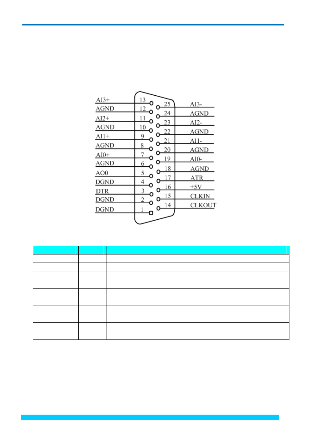
3.1 Analog Input/Output Connector..............................................................................................................................6
3.2 Digital Input Connector ..........................................................................................................................................7
3.3 Digital Output Connector........................................................................................................................................7
Chapter 4 Each Signal Connection Method..........................................................................................................................8
4.1 Analog Input Connection ........................................................................................................................................8
4.2 Analog Output Connection......................................................................................................................................9
4.3 Trigger Signal Connection ......................................................................................................................................9
4.4 Digital Input Connection.........................................................................................................................................9
4.5 Digital Output Connection ....................................................................................................................................10
4.6 Frequency Measurement Connection....................................................................................................................10
4.7Methods of Realizing the Multi-card Synchronization ..........................................................................................10
Chapter 5 The Instruction Trigger Function.......................................................................................................................12
5.1 Internal Trigger Mode ...........................................................................................................................................12
5.2 External Trigger Mode ..........................................................................................................................................12
5.3 AD Internal and External Clock Function.............................................................................................................14
5.3.1 Internal Clock Function of AD...................................................................................................................14
5.3.2 External Clock Function of AD..................................................................................................................14
5.4 Frequency Measuring Principium.........................................................................................................................14
5.4.1 PWM Principium .......................................................................................................................................14
5.4.2 Frequency Count Principium .....................................................................................................................15
Chapter 6 Note and Warranty Policy..................................................................................................................................16
6.1 Notes .....................................................................................................................................................................16
6.2 Analog Signal Input Calibration............................................................................................................................16
6.3 Analog Signal Output Calibration.........................................................................................................................16
6.4Warranty Policy......................................................................................................................................................16
Products Rapid Installation and Self-check ........................................................................................................................18
Rapid Installation ........................................................................................................................................................18
Self-check ...................................................................................................................................................................18
Delete Wrong Installation ...........................................................................................................................................18
BUY ONLINE at art-control.com/englishs or CALL+86-10-62991792-609 (CN) 1

PCI8025DataAcquisitionCard V7.002
Chapter 1 Overview
In the fields of Real-time Signal Processing, Digital Image Processing and others, high-speed and high-precision data
acquisition modules are demanded. ART PCI8025 data acquisition module, which brings in advantages of similar
products that produced in china and other countries, is convenient for use, high cost and stable performance.
ART PCI8025 is a data acquisition module based on PCI bus. It can be directly inserted into IBM-PC/AT or a computer
which is compatible with PCI8025 to constitute the laboratory, product quality testing center and systems for different
areas of data acquisition, waveform analysis and processing. It may also constitute the monitoring system for industrial
production process.
Unpacking Checklist
Check the shipping carton for any damage. If the shipping carton and contents are damaged, notify the local dealer or
sales for a replacement. Retain the shipping carton and packing material for inspection by the dealer.
Check for the following items in the package. If there are any missing items, contact your local dealer or sales.
¾PCI8025 Data Acquisition Board
¾ART Disk
a) user’s manual (pdf)
b) drive
c) catalog
¾Warranty Card
FEATURES
Analog Input
¾converter type: AD7899-1 (compatible with AD7899-2)
¾Input Range:
AD7899-1: ±1.25V, ±2.5V, ±5V, ±10V
AD7899-2: 0~2.5V, 0~5V
¾14-bit resolution
¾Sampling Rate: The maximum sampling rate of asynchronous is 1.6MHz (0.625 ms/point)
The minimum sampling rate of asynchronous is 0.04Hz (about 25s/point)
The maximum sampling rate of synchronous is 400KHz/ch (2.5ms/point)
The minimum sampling rate of synchronous is 0.01Hz/ch (100s/point)
Note: The actual channel sampling rate = sampling rate / number of sampling channels (asynchronous sampling)
The actual channel sampling rate = sampling rate (Synchronous sampling)
Frequency Formula: sampling frequency= main frequency/the number of frequency division, main frequency =
80MHz, 32-bit frequency division, the number of frequency division range: 200~232.
¾Input Channels: 4 channels
¾Channel Switching Mode: 4-channel 4-chip work independently
¾Data Read Mode: software inquiry and DMA mode
¾Memory Depth: 64K word RAM memory
¾AD Mode: asynchronous and synchronous
¾Clock Source: internal clock, external clock (software configuration)
¾Trigger Mode: software trigger, hardware trigger (external trigger)
BUY ONLINE at art-control.com/englishs or CALL+86-10-62991792-609 (CN) 2

PCI8025DataAcquisitionCard V7.002
¾Trigger Type: level trigger, edge trigger
¾Trigger level: 4,096 software adjustable, trigger level achieved by the analog output AO0
¾Analog trigger source software selectable: AI0, AI1, AI2, AI3, ATR
¾Analog trigger source (ATR) input range: ±15V
¾Programmable Gain: 1 time
¾Analog Input Impedance: 10MΩ
¾Analog input common-mode voltage range: <± 2V
¾Non-linear error: ±1LSB(Maximum)
¾System Measurement Accuracy: 0.05%
¾Operating Temperature Range: 0℃~50℃
¾Storage Temperature Range: -20℃~70℃
Analog Output
¾Output Range: ±10V, ±5V, 0~10V, 0~5V
¾12-bit resolution
¾Set-up Time: 10μs (0.01%)
¾Update Rate: The maximum update rate is 100KHz (10us/points)
The minimum sampling rate decided by the user software
¾Channel No.: 1-channel
¾Output Impedance: 0.2Ω
¾Non-linear error: ±1LSB(Maximum)
¾Output Error (full-scale): ±1LSB
¾Operating Temperature Range: 0℃~50℃
¾Storage Temperature Range: - 20℃~70℃
Digital Input
¾Input channels: 16
¾Electronic standard: TTL compatible
¾Maximum Sink Current: less than 0.5mA
¾High level: ≥2V
¾Low level: ≤0.8V
Digital Output
¾Output channels: 16
¾Electronic standard: CMOS compatible
¾Maximum drop-down current: 20mA
¾Maximum pull-up current: 2.6mA
¾High level: ≥3.4V
¾Low level: ≤0.5V
Frequency Measurement Function
¾Frequency Measurement Types: pulse width measurement frequency (analog frequency measurement), counting
measurement frequency (digital measurement frequency)
¾Pulse Direction: negative pulse, positive pulse, either negative or positive pulse
¾Trigger Source: ATR, AI0, AI1, AI2 and AI3 (pulse-width measurement frequency parameters)
¾Trigger Level: <±15V (pulse-width measurement frequency parameters)
BUY ONLINE at art-control.com/englishs or CALL+86-10-62991792-609 (CN) 3

PCI8025DataAcquisitionCard V7.002
¾Counter Timing: <107S (digital measurement frequency parameters)
Other Features
¾Board Clock Oscillation: 40MHz
¾Board Dimension: 183mm (L) * 100mm (W)*13.50mm (H)
BUY ONLINE at art-control.com/englishs or CALL+86-10-62991792-609 (CN) 4

PCI8025DataAcquisitionCard V7.002
Chapter 2 Components Layout Diagram and a Brief Description
2.1 The Main Component Layout Diagram
2.2 The Function Description for the Main Component
2.2.1 Signal Input and Output Connectors
CNI: Analog signal input and output connector
P1: Digital input port
P2: Digital output port
2.2.2 Potentiometer
RP20, RP26, RP28, and RP32: Analog input 0, 1, 2, 3 channels zero-point adjustment potentiometer
RP25, RP26, RP31, and RP33: Analog input 0, 1, 2, 3 channels full-scale adjustment potentiometer
VR_-1.25: adjust the DA converter -1.25V reference voltage
VR-DA: Analog output full-scale adjustment potentiometer
VAR9: Analog output zero-point adjustment potentiometer
BUY ONLINE at art-control.com/englishs or CALL+86-10-62991792-609 (CN) 5

PCI8025DataAcquisitionCard V7.002
Chapter 3 Signal Connectors
3.1 Analog Input/Output Connector
CN1: 25-pin D-type
Pin definition
Name Color Description
AI0+~AI3+ Input
The positive of analog differential input signals
AI0-~AI3- Input
The negative of analog differential input signals
AO0 Output
Analog output
AGND GND
Analog ground
DGND GND
Digital ground
ATR Input
External trigger signal (analog), reference ground is AGND.
DTR Input
Counting measurement frequency, reference ground is DGND.
+5V Output
Output 5V, supply 100mA(max)
CLKIN Input
External clock input, reference ground is DGND.
CLKOUT Output
Internal clock output, reference ground is DGND.
BUY ONLINE at art-control.com/englishs or CALL+86-10-62991792-609 (CN) 6

PCI8025DataAcquisitionCard V7.002
3.2 Digital Input Connector
20-pin definition
Pin Name Direction Description
DI0~DI15 Input Digital input.
DGND GND Digital ground.
+5V Output
Output 5V, supply 100mA(max)
3.3 Digital Output Connector
Pin Name Direction Description
DO0~DO15 Output Digital output.
DGND GND Digital ground.
+5V Output
Output 5V, supply 100mA(max)
BUY ONLINE at art-control.com/englishs or CALL+86-10-62991792-609 (CN) 7

PCI8025DataAcquisitionCard V7.002
Chapter 4 Each Signal Connection Method
4.1 Analog Input Connection
Single-ended mode can achieve a signal input by one channel, and several signals use the common reference ground.
This mode is widely applied in occasions of the small interference and relatively many channels.
AGND
AI0+
AI0-
+
Device
Analog signal
AI1+
AI1-
+
Device
AI3+
AI3-
+
Device
_
_
_
Figure 4.1 single-ended input connection
Double-ended input mode, which was also called differential input mode, uses positive and negative channels to input a
signal. This mode is mostly used when biggish interference happens and the channel numbers are few.
Single-ended/double-ended mode can be set by the software, please refer to PCI8025 software manual.
According to the diagram below, PCI8025 board can be connected as analog voltage double-ended input mode, which
can effectively suppress common-mode interference signal to improve the accuracy of acquisition. Positive side of the
8-channel analog input signal is connected to AI0+~AI3+, the negative side of the analog input signal is connected to
AI0-~AI3-, equipments in industrial sites share the AGND with PCI8025 board.
Figure 4.2 Differential-ended input mode
BUY ONLINE at art-control.com/englishs or CALL+86-10-62991792-609 (CN) 8

PCI8664 Data Acquisition Card
4.2 Analog Output Connection
Figure 4.3 analog signal output connection
4.3 Trigger Signal Connection
4.4 Digital Input Connection
DI1
DI2
DI15
DGND
DI0
BUY ONLINE at art-control.com/englishs or CALL+86-10-62991792-609 (CN) 9
Tabla de contenidos
Otros manuales de Registrador de datos de ART Technology Development


