List of Figures
List of Figures
Figure 1.1 – 7224 Front Panel.............................................................................................................6
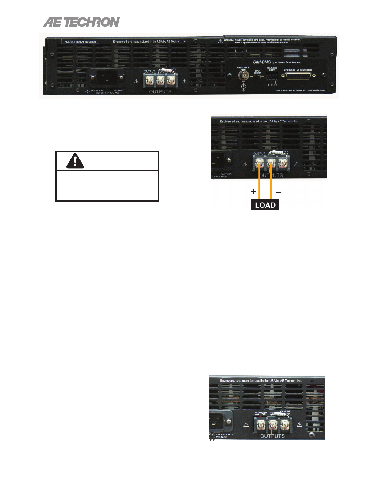
Figure 2.1 – 7224 Back Panel .............................................................................................................8
Figure 2.2 – Connecting the Load .......................................................................................................8
Figure 2.3 – Closeup of the Output Terminals .....................................................................................8
Figure 2.4 – Closeup of SIM card........................................................................................................9
Figure 2.5 – Wiring for Unbalanced or Balanced Input Connector......................................................9
Figure 2.6 – Closeup of AC Mains Outlet ..........................................................................................10
Figure 2.7 – Sample of Congurations Setting Label........................................................................10
Figure 3.1 – Power Switch.................................................................................................................11
Figure 3.2 – Gain Control ..................................................................................................................11
Figure 3.3 – Push Buttons.................................................................................................................11
Figure 3.4 – Indicators.......................................................................................................................12
Figure 3.5 – Main Status Indicators for Stand-Alone Ampliers ........................................................12
Figure 3.6 – Fault Status Indicators for Stand-Alone Ampliers ........................................................13
Figure 3.7 – Main Status Indicators for Multi-Amplier Systems.......................................................14
Figure 3.8 – Fault Status Indicators for Multi-Amplier Systems.......................................................15
Figure 3.9 – Back Panel Controls and Connectors ...........................................................................17
Figure 4.1 – Access Panel Screw Locations .....................................................................................18
Figure 4.2 – Main Board Location Inside Access Panel ....................................................................19
Figure 4.3 – Master/Slave Setting .....................................................................................................19
Figure 4.4 – Gain Trim Control ..........................................................................................................19
Figure 4.5 – Controlled-Voltage/Controlled-Current Mode Setting ....................................................20
Figure 4.6 – Compensation Setting...................................................................................................20
Figure 4.7 – Run Mode/Stop Mode on Power-Up Setting .................................................................20
Figure 4.8 – Standby Mode on Over Temp Setting ...........................................................................21
Figure 4.9 – Standby Mode on Over Load Setting ............................................................................21
Figure 4.11 – Location of Amplier High-Voltage Transformer Sockets ............................................22
Figure 4.10 – Accessing the Power Supply Board ............................................................................22
Figure 4.12 – J3 and J7 Plug Locations for High-Current Output......................................................22
Figure 4.13 – J4 and J8 Plug Locations for High-Voltage Output .....................................................22
Figure 4.14 – Bi-Level Power Switch Location..................................................................................23
Figure 5.1 – Remote Status and Control Pinouts..............................................................................24
Figure 5.2 – Remote Run/Standby Monitor.......................................................................................24
Figure 5.3 – Remote Status and Reset Schematic ...........................................................................25
Figure 5.4 – Remote Enable/Standby ...............................................................................................26
Figure 5.5 – Remote Voltage Monitoring ...........................................................................................27
Figure 5.6 – Remote Current Monitoring...........................................................................................27
Figure 5.7 – Remote Current Monitoring, Alternate Method..............................................................28
Figure 5.8 – Input to Output Comparison, Controlled-Voltage Operation..........................................28
Figure 5.9 – Input to Output Comparison, Controlled-Current Operation..........................................29
Figure 5.10 – Factory-installed Default RC Network .........................................................................29
Figure 5.11 – Custom Compensation Location .................................................................................31
Figure 5.12 – Compensation Effects on Waveform ...........................................................................31
Figure 5.13 – Square Wave Showing a Decrease in R is Required..................................................32
Figure 5.14 – Square Wave Showing an Increase in R is Required .................................................32
Figure 5.15 – Square Wave Showing an Increase in C is Required .................................................32
Figure 6.1 – Board-Level Functional Block Diagram.........................................................................37
Figure 8.1 – +Vcc and –Vcc Point Locations.....................................................................................39
Figure 8.2 – Fuse F1 Location...........................................................................................................40
Figure 8.3 – Interlock I/O Connector .................................................................................................40
Figure 9.1 – Voltage Potential vs. Frequency....................................................................................45
Figure 9.2 – Frequency Response ....................................................................................................45
Figure 9.3 – Noise vs. Frequency......................................................................................................45
Figure 9.4 – Continuous Power vs. Frequency .................................................................................45
Figure 9.5 – Thermal Performance....................................................................................................45
Figure 9.6 – DO 160 Section 18.2 AC Power Processing .................................................................45
Figure 9.7 – DC Current Over Time at 13.5 VDC ..............................................................................46
Figure 9.8 – DC Current Over Time, 2-ohm Load .............................................................................46
Figure 9.9 – DC Current Over Time, 3-ohm Load .............................................................................46
Figure 9.10 – DC Current Over Time, 4-ohm Load ...........................................................................46
Figure 9.11 – DC Current Over Time, Comparison with 4-ohm Load................................................46