Rohm BD8628EFV Hoja de especificaciones

TECHNICAL NOTE
System Power Supply for TV Series
Built-in 1ch FET
Synchronous Rectification Type
DC/DC converters
BD8628EFV, BD8624EFV
●Description
BD8628EFV / BD8624EFV have realized the high performance and reliability required as a power supply for thin-screen TV.
With built-in FET 1ch current mode control, the DC/DC Converter series has the advantage of high-speed load response and wide
phase margin.
Due to the high-speed load response, it is most suitable for TV-purpose processors with increasingly high performance, and due to the
wide phase margin it leaves a good margin for board pattern & constant setting and so facilitates its application design.
As a high-reliability design, it has various built-in protection circuits (overcurrent protection, output voltage abnormal protection, thermal
protection, and off-latch function at the time of abnormality etc.), therefore as an advantage it does not easily damage in every possible
abnormal condition such as all-pin short circuit test etc. and hence most suitable for thin-screen TV which requires the high reliability.
●Features
1) 1ch synchronous rectification step-down system DC/DC converter
2) Soft start, soft off function
3) Built-in low voltage / overvoltage protection function
4) Built-in overcurrent protection function
5) Frequency setting by external resistance is available. (RT terminal)
6) Protection time setting by external resistance is available. (RSET terminal)
7) Built-in RT / RSET terminal open/short protection function
8) Protection control with built-in sequencer
9) Built-in adjustment function time of off latch
10) Built-in error state detection signal output function
11) Built-in tracking function
12) Corresponded to protecting bus
13) Load current Maximum 3A
14) HTSSOP-B24 Package
Aug. 2008

2 / 14
●Electric characteristic
(Ta=25℃, VCC=6.5V, GND=0V,CTL=6.5V unless otherwise specified.)
Parameter Symbol specification value UNIT Condition
MIN TYP MAX
Circuit current 1 IQ1 - 0 10 μA CTL=0V
Circuit current 2 IQ
2
- 3.4 - mA CTL=VCC
< Error amplifier part >
Standard voltage (VREF)V
RE
F
0.792 0.8 0.808 V Terminal FB and FC terminal short
Terminal FB Input bias current IFBB -1 0 1 μA VFB=0.9V
Terminal FC Clamping voltage H VFCH 1.8 - - V VFB=0.7V
Terminal FC Clamping voltage L VFCL - - 0.2 V VFB=0.9V
Terminal FC Sink current IFCSINK 0.5 - - mA VFB=0.9V, VF
C
=0.4V
Terminal FC Source current IFCSOURCE - - -70 μA VFB=0.7V, VF
C
=1.6V
Open loop gain AVER
R
- 100 - dB
<OSC part>
Oscillation frequency FOSC 400 500 600 kHz
When terminal RT 27kΩis
connected
<Soft start >
Charging current ISS -3 -2.5 -2 μA VSS=1.0V
Terminal SS Threshold voltage VSSTH 0.98 1.08 1.18 V VSS Volta
g
e
Terminal SS Clamping voltage VSSCLM 2.2 2.4 - V
Terminal SS Standby voltage VSSSTB 0.1 0.15 - V VSS Volta
g
e(L→H)
Terminal SS Discharge resistance RSS 49 70 91 kΩCTL=0V
Terminal SS Protection circuit start voltage VSSPON 1.0 1.1 1.2 V VSS Volta
g
e(L→H)
Terminal SS Protection circuit start voltage
Maximum hysteresis error VSSPON_HYS 10 100 200 mV VSS Voltage
< Low voltage, over voltage detection part>
Terminal FB Low voltage detection voltage VLV
P
0.51 0.56 0.61 V VFB Volta
g
e
Terminal FB Overvoltage detection voltage VOV
P
0.86 0.96 1.06 V VFB Volta
g
e
< Over current detection part>
Output current limitation threshold Ilm
t
VCC-0.9 VCC-0.7 VCC-0.5 V VSW Volta
g
e
<Power MOS>
Upper side MOS ON resistance RONU - 110 - mΩV
BOOT-VSW =5V
Lower side MOS ON resistance R
O
NL - 110 - mΩV
VREG
5
=5V
<Others>
Terminal PDET L output voltage VOL
_
P
DET - - 0.4 V IOL=100uA
Terminal CTL input voltage H level voltage VIH_CTL 2.0 - VCC V CTL terminal
Terminal CTL input voltage L level voltage VIL
_
CTL - - 0.5 V CTL terminal
Terminal CTL input current II
_
CTL - 60 90 μA CTL terminal, CTL=VCC
VFB : FB terminal voltage, VFC : FC terminal voltage, VSS : SS terminal voltage, VMONVCC : MONVCC terminal voltage
Not designed for radiation resistance.
Current capability should not exceed Pd.

3 / 14
Permissible loss
This package is a product of which the feature is the high heat radiation, and connect the back to GND
based on recommended land pattern when you mount.
Permissible loss : Pd [W]
ROHM standard substrate specification
Material 4 layer glass epoxy substrate(back copper foil70mm×70mm)
Size 70mm×70mm×1.6mmt(Sarmalbiaing is in the substrate.)
Figure 1 Heat decrease curve
※These values are the actual measurement values, and no guarantee values.
θ
jc
[
℃
/W]
θ
j
a
[
℃/W]
T
STGmin
[
℃
]
T
STGma
x
[
℃]
T
a min
[℃]
T
a ma
x
[
℃]
T
cma
x
[
℃]
T
j
ma
x
19.0 31.3 -50.0 150.0 -45.0 85.0 150.0 150.0
Destruction
temperature
[
℃]
Destruction
temperature

4 / 14
●Block diagram
SEQ
Control
VREF
OVP
LVP
OSC
Driver
Control
17
4
6
PROTECT
BUS
I/F
RT
OPEN/SHORT
CTL
10
time
VCC
RT
RSET
PDET
PIO
CTL
SW
SW
PGND
PGND
TEST1
TEST2
PVCC
PVCC
BOOT
VREG5
FC
FB
SS
GND
9 8 7 5
18 19
3
OSC
OSC
VREG5
2 1
N.C.
N.C.
N.C.
N.C.
Figure-2 Block diagram・Application diagram
●Terminal explanation
No. Symbol Description No. Symbol Description
1 PGND Power GND terminal 13 RT
Frequency adjustment resistance connection terminal
2 PGND Power GND terminal 14 RSET
Off latch effective time adjustment resistance terminal
3 N.C. No wire connection.
(Connect to GND. ) 15 PDET Error state notification terminal
4 N.C No wire connection.
(Connect to GND. ) 16 PIO Error state notification
and external IC error detection terminal
5 SW SW terminal 17 CTL Enable input
6 SW SW terminal 18 VCC VCC power supply terminal
7 BOOT High side Power MOS gate drive
power source terminal 19 PVCC Power VCC terminal
8 VREG5 Internal power supply (5.0V) output terminal 20 PVCC Power VCC terminal
9 GND GND 21 TEST2 Test terminal (Connect to GND. )
10 FC Phase amends terminal 22 TEST1 Test terminal (Connect to GND. )
11 FB Feedback terminal 23 N.C. No wire connection.
(Connect to GND. )
12 SS
Soft start adjustment capacity connection terminal 24 N.C. No wire connection.
(Connect to GND. )
※Please give to VCC+0.3V as an operation condition in all input terminals except the terminal BOOT.
However, please do not exceed the absolute maximum rating as VCC=PVCC.
Table 1 Terminal explanation
5 / 14
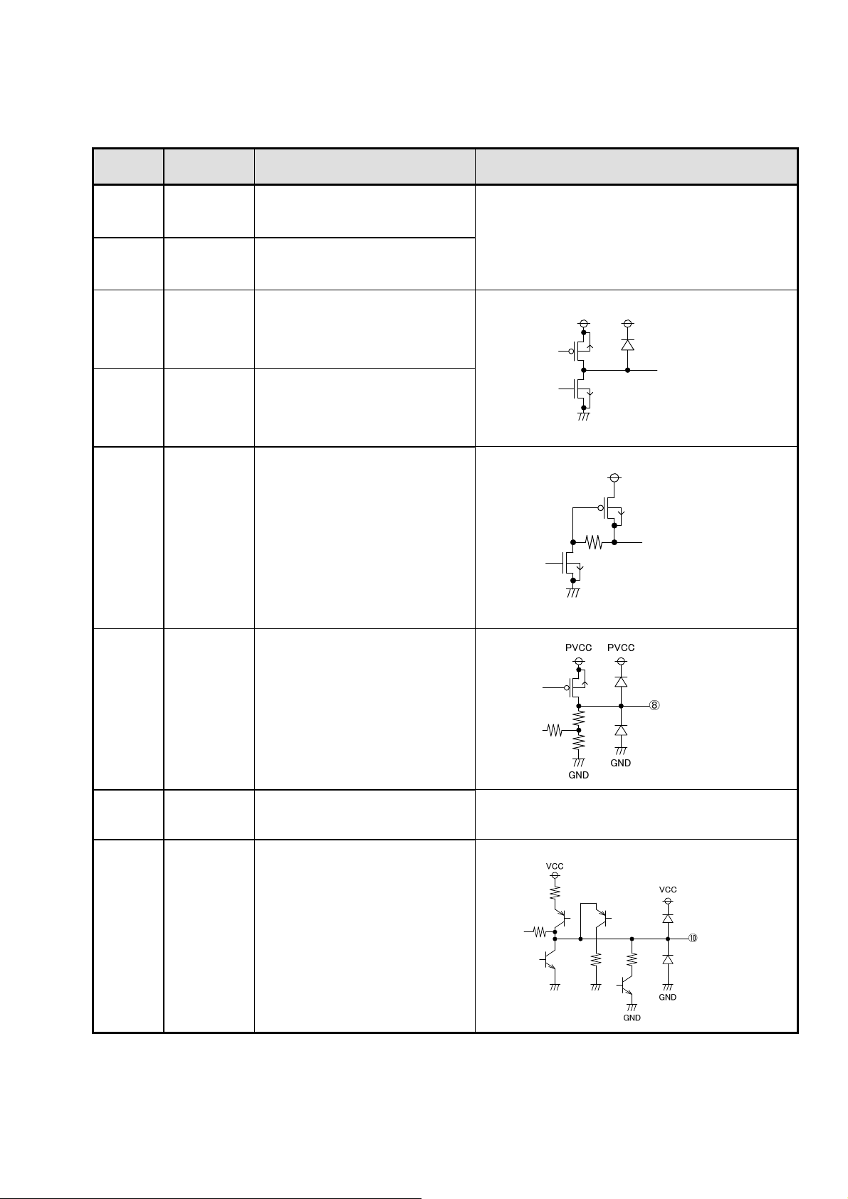
●Terminal equivalent circuit chart
Terminal
No.
Terminal
name Explanation Terminal equivalent circuit chart
1 PGND
Power GND
(The same potential as the GND
terminal)
2 PGND
Power GND
(The same potential as the GND
terminal)
5 SW SW terminal
6 SW SW terminal
7 BOOT High side Power MOS gate drive power source
terminal
8 VREG5 Internal power supply (5.0V) output terminal
9 GND GND
10 FC Phase amends terminal
PVCC PVCC
PGND
⑤
⑥
VREG5
PGND
⑦

6 / 14
Terminal
No.
Terminal
name Explanation Terminal equivalent circuit chart
11 FB Voltage detection terminal
12 SS Soft start adjustment capacity connection
terminal
13 RT Frequency adjustment resistance connection
terminal
14 RSET Off latch effective time adjustment resistance
terminal
15 PDET Error state notification terminal
VCC
GND
⑪
VCC

7 / 14
Terminal
No.
Terminal
name Explanation Terminal equivalent circuit chart
16 PIO Error state notification and external IC error
detection terminal
17 CTL Enable input
21 TEST2 Test terminal (Connect to GND. )
22 TEST1 Test terminal (Connect to GND. )
19 PVCC Power VCC terminal
20 PVCC Power VCC terminal

8 / 14
●Operation description
ON/OFF control
DC/DC converter ON/OFF function
DC/DC converter controller can be controlled ON/OFF by CTL terminal.
Analog circuit starts operation at ON control (on mode), and goes down to setting output voltage.
Analog circuit should be standby at OFF control (off mode), and output voltage becomes 0V.
Table1 DC/DC converter ON/OFF function
C
TL terminal voltage
>VIHCTL ON control
<VILCTL
O
FF contro
l
Soft start time set function
DC/DC converter can do soft start without overshoot by charging soft start capacity (Css) connected between SS
terminal and GND by charging current at ON control.
The mute of the output is released when it reaches VSS=0.15V (VSSSTB), and the output voltage does the soft start
operation from the point of VSS=0.3V (typ) in proportion to the voltage of the terminal SS.
Also, soft start time (tss) can be set by setting soft start capacity arbitrarily.
Soft start time (tss) should be set at 3msec < tss < 30msec.
※Please note that the overshoot is not caused in the output setting voltage when setting it to tss≦3msec.
SS
ISS
C
SSTH
V
SS
t
Discharge function
DC/DC converter can do soft off by discharging load discharged to soft start capacity connected between SS terminal
to GND by discharging resistance at OFF control.
Soft off operates in proportion to the voltage of the terminal SS the output voltage from the point of VSS=0.8V (typ).
Figure 2 Wave form at ON/OFF control

9 / 14
OSC oscillation frequency setting function
SW output oscillation frequency of DC/DC converter can be set by installing resistance between RT terminal and GND
externally.
Figure 3 Terminal RT resistance-oscillation frequency
Range of terminal RT connection resistance setting
23kΩ≦Rrt≦135kΩ
(100kHz≦fosc≦600kHz)
1
0
10
0
100
0
1000
0
11
0
10
0
100
0
RT terminal resistance[KΩ]
Switching frequency [KHz]
*Reference date

10 / 14
PROTECT BUS Input/output function
The terminal PIO is PROTECT BUS Input/output terminal. The terminal PIO is Hi-Z when DC/DC usually operates. When the
terminal PIO becomes LOW by connecting PROTECT BUS, DC/DC is turned off. Afterwards, when the terminal PIO becomes
HIGH, it reactivates.
DC/DC is Off latch when DC/DC error detects it and the terminal PDET becomes LOW.
Table2 PIO terminal, PDET terminal output function
DC/DC
Error detection PIO terminal PDET terminal DC/DC
Undetection Hi-Z Hi-Z ON
Undetection LOW Hi-Z OFF
Detection LOW LOW Off latch
PROTECT BUS Timing chart
If two or more BD8628EFV/BD8633EFV/BD8624FV/BD8630FV is connected in PROTECT BUS, and it uses at the same time,
when one IC error detects, all remaining IC becomes PIO = Low at the same time, and the output is turned off.
Protecting BUS part timing chart
IC_A
PDET
IC_A
PIO
High
OFF LATCH
When two or more BD8628EFV/BD8633EFV/BD8624FV/BD8630FV is used at the same time,
If one IC error detects, all IC becomes DC/DC OFF at the same time.
IC_B
PIO
DC/DC OFF
IC_B
PDET
IC_A detects error.
IC_B
Vo
High
High
High
LOW
LOW
LOW
0V
PIO
IC_A
PIO
IC_B
Este manual sirve para los siguientes modelos
1


