Koheron Alpha250 Manual de usuario

Alpha250 User Guide
Koheron Alpha250 250 MSPS acquisition board
Getting started
Warnings
The Alpha250 power supply must be turned off before connecting or disconnecting:
the micro-SD card
peripherals on the expansion connector
Turn on the board
First, insert the micro-SD card into the micro-SD slot. Then connect the 12V jack of
the power supply. The power good green LED (PWGD) and the FPGA done orange
LED (DONE) indicate the system has correctly started.
Communicating with the board
LAN
The ethernet port is the main communication interface with the Alpha250. It can be
connected to a local network via a router or directly to a computer. The last 8 bits of
the IP address are displayed on the 8 user LEDs.
Serial interface
The serial UART debugging interface can be accessed by the micro USB connector.
1 / 13
www.koheron.com

The required steps are described here.
Connectors
Alpha250 connectors
12 V external power supply
The external supply connector is a jack with 1.95 mm center pin and 6 mm outer
diameter. Only 12 V must be supplied on this connector. Running the Alpha250
requires at least 1 A. More current may be required depending on the load on the
expansion connector. Maximum current is 3 A (protected by an electronic fuse).
USB 2.0
This is a USB 2.0 host connector. It provides up to 1 A current at 5 V (shared with the
5 V supply of the expansion connector). The power and data pins are ESD protected.
Micro USB 2.0
Connects to the UART0 PS core via a FTDI device. It is used as a debugging serial
interface. The power and data pins are ESD protected.
Gigabit ethernet
The Alpha250 is capable of 10/100/1000 Mbit Ethernet.
2 / 13
www.koheron.com

MicroSD card
The micro SD card is connected to the SD0 PS core via a level-shifter. The SD card
I/Os are ESD protected.
Expansion connector
Alpha250 expansion connector
It contains:
Power supplies. 12 V from external supply. 5 V up to 1 A (shared with USB 2.0
connector). + 3.3 V up to 800 mA, sequenced with I/Os supply. - 3.3 V up to
500 mA.
A dedicated I2C bus I2C1 with interrupt.
16 single ended or 8 differential I/Os EXP_IOx. They are connected to the FPGA
Bank 35. Voltage level is 3.3 V. All I/Os are ESD protected. Warning: These pins
are connected directly to the Zynq SoC and must be driven from VCCIO_3V3
both for voltage compliance and power sequencing. Applying non compliant
voltages on these pins may result in SoC failure.
Two LVDS clocks from the clocking subsystem EXP_CLK0 and EXP_CLK1.
4 user IOs from the GPIO expander USER_IOx. Voltage level is 3.3 V. They can
be configured as inputs or outputs, open-drain or pull-up. These I/Os have 22
3 / 13
www.koheron.com

Ω series protection resistors. They are ESD protected.
A 2.5 V voltage reference. This reference acts as a ratiometric tracking with the
reference used for all the data converters (RF ADC, RF DAC, precision ADC,
precision DAC). It delivers up to 150 mA (Care must be taken with the voltage
drop in track resistance at large currents).
4 precision ADC inputs. Differential inputs to the precision 24-bit ADC.
4 precision DAC outputs. Outputs from the 16-bit precision DAC.
Subsystems
RF ADC
The RF Analog-to-Digital Converter has 2 acquisition channels with 14-bit resolution
and 250 Msps maximum sampling rate (Linear Technologies LTC2157-14). It has two
inputs labeled IN0 and IN1 on the SMA connectors. The inputs are DC coupled and
50 Ω terminated. The optimum DC offset is reached when the input is driven from a
50 Ω output impedance source. The peak-peak input range is 1 Vpp (between -500
and 500 mV). The inputs are protected by a transient voltage suppressor clamping
over-voltages beyond ± 8 V.
Alpha250 RF ADC interface.
The encoding clock of the ADC is provided by the RF_ADC_CLK of the clocking system.
The output data are interfaced to the I/O Bank 34 of the FPGA. It consists of 14
LVDS pairs operating in double data rate. The maximum transfer rate per LVDS pair is
thus 500 Msps. The transfer protocol is described in the LTC2157-14 datasheet. A
clock synchronous with the data ADC_CLKOUT is also connecting the Bank 34.
The RF ADC is configured by the configuration SPI bus. The source code of the
corresponding C++ driver is on GitHub.
RF DAC
The RF Digital-to-Analog Converter has 2 outputs with 16-bit resolution and 250
Msps maximum sampling rate (Analog Devices AD9747). The outputs are labeled
OUT0 and OUT1 on the SMA connectors. Output impedance is 50 Ω. The outputs
are protected by a transient voltage suppressor clamping over-voltages beyond ± 8
V.
The output range is 1.5 Vpp maximum in a 50 Ω load. It can be adjusted using the
4 / 13
www.koheron.com
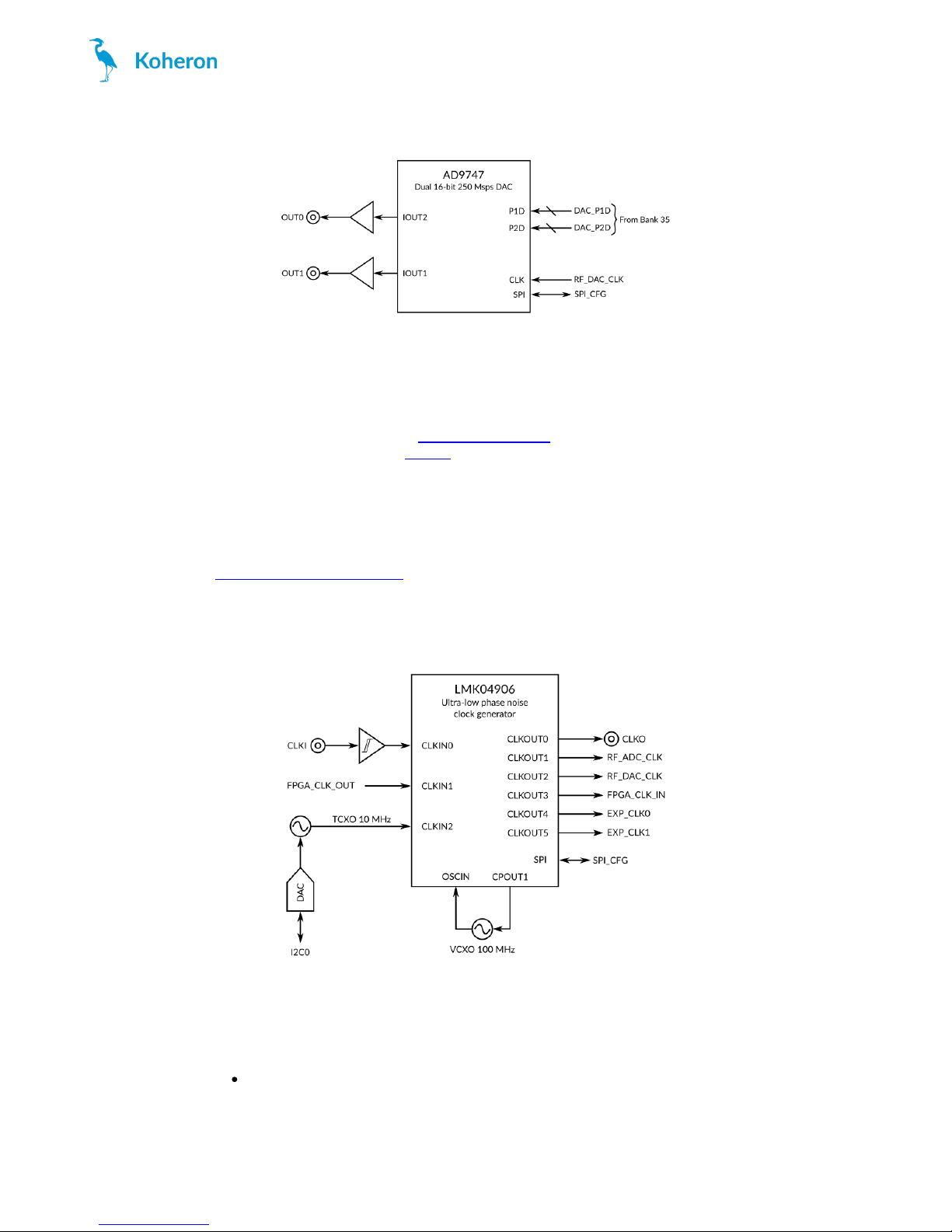
DAC gain on the configuration SPI bus. In the default configuration, the DAC outputs
1 Vpp in a 50 Ω load.
Alpha250 RF DAC interface.
The sampling clock of the DAC is provided by the RF_DAC_CLK of the clocking system.
The input data lines are interfaced to the I/O Bank 35 of the FPGA. It consists of 32
single-ended lines at 3.3 V.
The RF DAC is configured by the configuration SPI bus. The source code of the
corresponding C++ driver is on GitHub.
Clocking
The clocking system is organized around the ultra-low phase noise clock generator
(Texas Instruments LMK04906). A dual PLL setup is used. The first loop locks an
ultra-low phase noise VCXO (ABLNO-V-100.000MHz) onto a reference clock. It
serves as a phase-noise cleaner for the reference clock. The second loop locks the
LMK04906 internal VCO (2.37 to 2.6 GHz) onto the VCXO. A set of clock dividers
allows to produce up to six clocks at desired frequencies.
Alpha250 clocking system.
The clock generator is designed to accept 10 MHz reference clocks.
The reference clock sources are:
The CLKI SMA input on the board. It is a 50 Ω impedance input that accepts an
AC voltage of up to 2.5 Vpp (10 dBm). It also supports up to 5 VDC. An onboard
precision high-speed comparator (890 Mbps) provides effective clock recovery.
5 / 13
www.koheron.com

It is ESD protected.
The FPGA_CLK_OUT signal to discipline the system on a clock provided by the
FPGA.
The onboard 10 MHz temperature compensated voltage controlled crystal
oscillator (TCVCXO). It has a tight stability (± 280 ppb over the industrial
temperature range -40 to +85 °C). Its aging is ± 1 ppm per year maximum. A
DAC controlled from the I2C0 bus can be used to precisely tune its frequency.
The clock generator produces the following clocks:
An LVCMOS clock available on the board CLKO SMA output. This output is
ESD protected.
RF ADC sampling clock RF_ADC_CLK distributed as an LVDS signal.
RF DAC sampling clock RF_DAC_CLK distributed as an LVDS signal.
FPGA_CLK_IN is an LVDS input clock on the FPGA.
EXP_CLK0 and EXP_CLK1 are LVDS clocks available on the expansion connector.
The clock generator is configured by the configuration SPI bus via the
ClockGenerator driver.
Precision ADC
The precision ADC is a 8-channel, 24-bit sigma-delta ADC with programmable gain
amplifier (Analog Devices AD7124-8). The inputs differential pairs can be used to
sense either floating or ground referenced signal. They also facilitate Kelvin sense
connections. Differential input voltage range is ± 1.25 V.
Alpha250 Precision ADC interface.
The first four channels are available on the expansion connector. The next four
channels monitor the offsets of the RF ADC and RF DAC.
Communication with the precision ADC is done through a dedicated SPI bus. The
precision ADC data can be retrieved using the PrecisionAdc driver.
Precision DAC
The precision DAC is a 4-channel, 16-bit DAC (Analog Devices AD5686).
The output voltage ranges from 0 to 2.5 V. It includes an output buffer that can
deliver up to 20 mA per channel. The outputs are ESD protected.
6 / 13
www.koheron.com

Alpha250 Precision DAC interface.
The four output channels are available on the expansion connector. Communication
with the precision DAC is done through a dedicated SPI bus via the PrecisionDac
driver.
Temperature sensors
The Alpha250 has two high-accuracy temperature sensors (TMP116) with an
accuracy of ± 0.2 °C over -10 °C to +85 °C. One sensor is placed near the voltage
reference (T0 highlighted in blue) to allow temperature compensation in high
precision measurements. The other one is placed between the clock generator and
the RF ADC which is close to the hottest point on the board (T1 highlighted in red).\
Alpha250 temperature sensors. Voltage reference in blue, board in red.
The Zynq temperature T2 is also monitored using the XADC on the FPGA. The
TemperatureSensor driver allows to retrieve the 3 above temperatures. For reliable
operation, make sure that T1 < 70 °C and T2 < 85 °C.
Power monitors
The Alpha250 includes two power monitors (Texas Instruments INA230). Two rails
are monitored: the external 12 V power supply and the clocking subsystem supply. In
both cases, the current shunt resistor is 10 mΩ. Both power monitors are accessible
on the I2C0 bus via the PowerMonitor driver.
7 / 13
www.koheron.com

EEPROM
The Alpha250 has a 64-kbit EEPROM (Microchip 24AA64T-I/MC). It is accessible on
the I2C0 bus via the Eeprom driver.
The EEPROM is divided into two parts. The lower addresses are used by Koheron to
store identification and calibration data. The higher addresses (above 0x1000) are for
user applications. The EEPROM map addressing is given in the table below.
Description Offset Range
Identifications 0x000 0x100
Precision DAC 0x100 0x100
RF ADC channel 0 0x200 0x100
RF ADC channel 1 0x300 0x100
Clock generator 0x400 0x100
RF DAC channel 0 0x500 0x100
RF DAC channel 1 0x600 0x100
Precision ADC 0x700 0x100
User application 0x1000 0x100
EEPROM map addressing.
Zynq I/Os
The Zynq XC7Z020-2CLG400I has 2 I/O banks for the programmable logic (Banks
34 and 35) with 48 IOs each. One bank (Bank 0) is dedicated to the processing
system with a multiplexed I/O (MIO) interface. The set of peripherals and interface
buses is depicted below.
Zynq peripherals and communication buses.
I/O constraints are defined in the ports.xdc file.
8 / 13
www.koheron.com

RF ADC parallel bus
The RF ADC is interfaced to the Bank 34 by a LVDS parallel bus. The data for each
ADC channel are transferred in double data rate on a 7 line sub-bus. The RF ADC
also provides a clock synchronous with the output data ADC_CLKOUT. The
configuration is performed via the configuration SPI bus.
# RF ADC (Bank 34)
set_property IOSTANDARD DIFF_HSTL_I_18 [get_ports adc_*]
set_property PACKAGE_PIN P19 [get_ports adc_clk_in_clk_n]
set_property PACKAGE_PIN N18 [get_ports adc_clk_in_clk_p]
# Channel 0
set_property PACKAGE_PIN U17 [get_ports {adc_0_n[0]}]
set_property PACKAGE_PIN T16 [get_ports {adc_0_p[0]}]
set_property PACKAGE_PIN Y19 [get_ports {adc_0_n[1]}]
set_property PACKAGE_PIN Y18 [get_ports {adc_0_p[1]}]
set_property PACKAGE_PIN P16 [get_ports {adc_0_n[2]}]
set_property PACKAGE_PIN P15 [get_ports {adc_0_p[2]}]
set_property PACKAGE_PIN W19 [get_ports {adc_0_n[3]}]
set_property PACKAGE_PIN W18 [get_ports {adc_0_p[3]}]
set_property PACKAGE_PIN P18 [get_ports {adc_0_n[4]}]
set_property PACKAGE_PIN N17 [get_ports {adc_0_p[4]}]
set_property PACKAGE_PIN W20 [get_ports {adc_0_n[5]}]
set_property PACKAGE_PIN V20 [get_ports {adc_0_p[5]}]
set_property PACKAGE_PIN U20 [get_ports {adc_0_n[6]}]
set_property PACKAGE_PIN T20 [get_ports {adc_0_p[6]}]
# Channel 1
set_property PACKAGE_PIN W13 [get_ports {adc_1_n[0]}]
set_property PACKAGE_PIN V12 [get_ports {adc_1_p[0]}]
set_property PACKAGE_PIN Y14 [get_ports {adc_1_n[1]}]
set_property PACKAGE_PIN W14 [get_ports {adc_1_p[1]}]
set_property PACKAGE_PIN P20 [get_ports {adc_1_n[2]}]
set_property PACKAGE_PIN N20 [get_ports {adc_1_p[2]}]
set_property PACKAGE_PIN R14 [get_ports {adc_1_n[3]}]
set_property PACKAGE_PIN P14 [get_ports {adc_1_p[3]}]
set_property PACKAGE_PIN W15 [get_ports {adc_1_n[4]}]
set_property PACKAGE_PIN V15 [get_ports {adc_1_p[4]}]
set_property PACKAGE_PIN T15 [get_ports {adc_1_n[5]}]
set_property PACKAGE_PIN T14 [get_ports {adc_1_p[5]}]
set_property PACKAGE_PIN Y17 [get_ports {adc_1_n[6]}]
set_property PACKAGE_PIN Y16 [get_ports {adc_1_p[6]}]
RF DAC parallel bus
The RF DAC is interfaced to the Bank 35 by a LVCMOS 3V3 parallel bus. The data
for each channel are transferred on a 16 line sub-bus. The configuration is performed
via the configuration SPI bus.
# RF DAC (Bank 35)
set_property IOSTANDARD LVCMOS33 [get_ports dac_*]
set_property DRIVE 8 [get_ports dac_*]
set_property IOSTANDARD LVCMOS33 [get_ports dac_*]
set_property DRIVE 8 [get_ports dac_*]
# Channel 0
set_property PACKAGE_PIN D18 [get_ports {dac_0[0]}]
set_property PACKAGE_PIN E17 [get_ports {dac_0[1]}]
set_property PACKAGE_PIN E19 [get_ports {dac_0[2]}]
set_property PACKAGE_PIN E18 [get_ports {dac_0[3]}]
set_property PACKAGE_PIN A20 [get_ports {dac_0[4]}]
set_property PACKAGE_PIN B19 [get_ports {dac_0[5]}]
9 / 13
www.koheron.com

set_property PACKAGE_PIN F17 [get_ports {dac_0[6]}]
set_property PACKAGE_PIN F16 [get_ports {dac_0[7]}]
set_property PACKAGE_PIN B20 [get_ports {dac_0[8]}]
set_property PACKAGE_PIN C20 [get_ports {dac_0[9]}]
set_property PACKAGE_PIN L17 [get_ports {dac_0[10]}]
set_property PACKAGE_PIN L16 [get_ports {dac_0[11]}]
set_property PACKAGE_PIN D20 [get_ports {dac_0[12]}]
set_property PACKAGE_PIN D19 [get_ports {dac_0[13]}]
set_property PACKAGE_PIN G18 [get_ports {dac_0[14]}]
set_property PACKAGE_PIN G17 [get_ports {dac_0[15]}]
# Channel 1
set_property PACKAGE_PIN F20 [get_ports {dac_1[0]}]
set_property PACKAGE_PIN F19 [get_ports {dac_1[1]}]
set_property PACKAGE_PIN J16 [get_ports {dac_1[2]}]
set_property PACKAGE_PIN K16 [get_ports {dac_1[3]}]
set_property PACKAGE_PIN G20 [get_ports {dac_1[4]}]
set_property PACKAGE_PIN G19 [get_ports {dac_1[5]}]
set_property PACKAGE_PIN K18 [get_ports {dac_1[6]}]
set_property PACKAGE_PIN K17 [get_ports {dac_1[7]}]
set_property PACKAGE_PIN H20 [get_ports {dac_1[8]}]
set_property PACKAGE_PIN J20 [get_ports {dac_1[9]}]
set_property PACKAGE_PIN M18 [get_ports {dac_1[10]}]
set_property PACKAGE_PIN M17 [get_ports {dac_1[11]}]
set_property PACKAGE_PIN H18 [get_ports {dac_1[12]}]
set_property PACKAGE_PIN J18 [get_ports {dac_1[13]}]
set_property PACKAGE_PIN G15 [get_ports {dac_1[14]}]
set_property PACKAGE_PIN H15 [get_ports {dac_1[15]}]
Configuration SPI bus
A shared SPI bus is dedicated to the configuration of the RF ADC, the RF DAC and
the clock generator. In the reference design, a HDL core is used for the
communication on this bus. The interface is described below.
Configuration SPI bus.
Constraint file
The configuration SPI bus pins are connected to Bank 34 with 1.8 V LVCMOS
signals.
# Configuration SPI (Bank 34)
set_property IOSTANDARD LVCMOS18 [get_ports spi_cfg_*]
set_property PACKAGE_PIN R17 [get_ports spi_cfg_sdo]
set_property PACKAGE_PIN R16 [get_ports spi_cfg_sdi]
set_property PACKAGE_PIN W16 [get_ports spi_cfg_sck]
set_property PACKAGE_PIN V16 [get_ports spi_cfg_cs_rf_adc]
set_property PACKAGE_PIN U12 [get_ports spi_cfg_cs_rf_dac]
set_property PACKAGE_PIN T12 [get_ports spi_cfg_cs_clk_gen]
10 / 13
www.koheron.com
Otros manuales para Alpha250
2
Tabla de contenidos
Manuales populares de Tarjeta PCI de otras marcas


Belkin
Belkin F5D7000F Manual de usuario

Pericom
Pericom PI7C7100 Manual de usuario

ADLINK Technology
ADLINK Technology cPCI-3548 Manual de usuario

Digium
Digium TE200 Series Manual de usuario

Allo.com
Allo.com 2nd Gen E1/T1/J1 Manual de usuario

Western Digital
Western Digital FireWire PCI Adapter Manual de usuario