Ezurio BISM2 Manual de usuario

www.ezurio.com
BISM2 Bluetooth™ Version 2.0 Serial Module
1. General Description
Ezurio’s BISM2 Bluetooth Serial Module is a fully integrated and qualified Class 1 Bluetooth solution
designed for lowest cost of integration and ownershi for designers wishing to incor orate Bluetooth
functionality into their roducts. The module is qualified to Bluetooth Version 2.0.
The BISM2 Bluetooth Serial Module is one of the most com act com lete Bluetooth solutions, making
it ideal to integrate into handheld devices. However a version of the BISM2 module is available that
retains the same board size, mounting holes and connector as the revious Bluetooth Module from
Ezurio, allowing users to access the im roved radio erformance and functionality without the need
for any cb modifications.
The BISM2 Module is based on Cambridge Silicon Radio’s BlueCore 04 chi set. The module contain
sall of the hardware and firmware for a com lete Bluetooth solution, requiring no further com onents.
The Module has an integrated, high erformance antenna which is matched with the Bluetooth RF and
baseband circuitry. The firmware integrated into the BC04 chi set im lements the higher layer
Bluetooth rotocol stack, u to and including the Generic Access Profile (GAP), Service Discovery
Profile (SDAP), Serial Port Profile (SPP), Dial U Networking Profile (DUN), Headset Profile (HSP),
Hands Free Profile (HFP), File Transfer Profile (FTP) and Audio Gateway. A virtual rocessor is used
within the BC04 to im lement an AT command rocessor. This interfaces to the host system over a
straight forward serial ort using an extensive range of AT commands. The AT command set abstracts
the Bluetooth rotocol from the host a lication, saving many months of rogramming and
integration time. It rovides extremely short integration times for data oriented cable re lacement
and voice a lications. A low cost develo ment system is available for fast roduct evaluation and
develo ment.
An alternative version of firmware is available that rovides rogramming su ort for multi- oint
a lications.
The Module can be configured so that it can be attached to a ‘dumb’ terminal or attached to a PC or
PDA for cable re lacement a lications.
In addition to the Bluetooth functionality, The BISM2 Module rovides access to 9 General I/O lines
and 2 analogue in ut and out ut lines. These can be configured to rovide connection to sim le
devices such as switches or LEDs without requiring any external rocessing. Both the GPIO and ADC
lines can be accessed either via the wired host UART connection, or remotely over the Bluetooth link.
The BISM2 module is su lied in a small form factor cb (22.0mm x 34.0mm x 7.6mm), that
connects to a main cb using a 40 way Hirose connector. The interface is com atible with the BISM1
module. The module includes a high sensitivity, high gain antenna which rovides excellent range.
Ty ical o en field erformance rovides ranges of over 250 metres at transmit owers of 4mW.
Su ort is rovided for low ower modes that make the BISM2 articularly a licable to battery
owered installations.
The BISM2 module is Lead-free and is RoHS com liant and su orts an industrial tem erature range
of -40°C to +85°C.
1.1 Applications
•POS Equi ment
•Medical Equi ment
•Telematics
•Voice A lications
•Industrial Automation
•Automotive A lications
Bluetooth is a trademark owned by Bluetooth SIG, Inc., USA, and is licensed to Ezurio Ltd
Module shown without RF shield

www.ezurio.com
2. Features
Feature Implementation
Bluetooth Transmission Class 1
Fully Bluetooth re-qualified Bluetooth 2.0
Range 250 metres ty ical (free s ace)
Frequency 2.400 – 2.485 GHz
Max Transmit Power +6dBm
Min Transmit Power -27dBm
Receive Sensitivity Better than -86dB
Data Transfer rate U to 300Kb s
Serial Interface RS-232 bi-directional for commands and data using AT commands
Serial arameters Default 9600,n,8,1 - Configurable from 1,200b s to 961,200 b s.
Su ort for DTR, DSR, DCD, RI, RTS, CTS
Physical size 22.8 x 33.8 x 7.6 mm, 8g
24.0 x 69.0 x 7.6mm, 9g (BISM1 Form Factor)
Current consum tion Ty ically 22mA during data transfer in standard ower mode. Lower
owers are attainable with a configurable low ower mode.
Low ower sniff mode 2.5mA ty
Tem erature Range Normal o eration: -40°C to +85°C
Su ly Voltage 3.6V – 7.0V
Brown-out Integrated brown out detection
Interface Levels 3.3V Logic
Audio Audio can be transferred over SCO channels through the PCM interface
at 64kb s. PCM can be configured as master or slave.
Profiles FTP Server, SPP, DUN, FTP, Audio Gateway, Headset, Handsfree
Multi oint Max 7 slaves
Field u gradeable Over UART
Protocols
Single oint firmware is controlled and configured using AT
Commands. Standard multi oint firmware uses a sim le acket based
rotocol and requires a host to enable the module to function
effectively.
Single oint only allows a oint to oint connection whereas multi oint
allows more than one simultaneous connection.
GPIO 9 x digital
2 x analogue (8 bit resolution)
Indicators 1 x rogrammable LED (small form factor board only)
Lead free Lead-free and RoHS com liant
www.ezurio.com
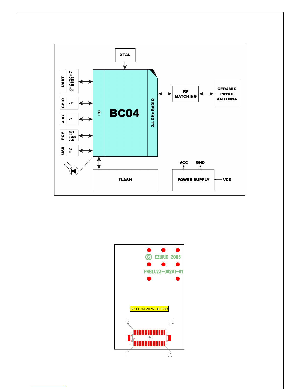
3. Functional Block Diagram
3.1 Connection Diagram
The Module is equi ed with a 40- in 0.5mm itch board-to-board connector that connects to the
a lication latform.
www.ezurio.com
3.2 Pin Descriptions
The Hirose DF12C board-to-board connector on the module is a 40- in double-row rece tacle.
The table below defines the in functions. Note that this in-out is as viewed from the underside of
the Module.
Pin
No.
Signal Description Pin
No.
Signal Description
1 Analogue 0 1.8v Max 2 GPIO1 I/O for Host.
3 Analogue 1 1.8v Max 4 GPIO2 I/O for Host
5 SPI_MISO SPI bus serial O/P 6 UART_RI ‘Ring’ In ut or Out ut
7 SPI_CSB SPI bus chi select I/P 8 UART_DCD In ut or Out ut
9 SPI_CLK SPI bus clock I/P 10 UART_DSR In ut
11 GND 12 GPIO3/UART_DTR
I/O for Host
13 RESET Reset I/P * 14 GPIO4 I/O for Host & LED
15 GND 16 GPIO5 I/O for Host
17 SPI_MOSI SPI bus serial I/P 18 GND
19 UART_CTS Clear to Send I/P 20 PCM_CLK PCM Clock I/P
21 UART_TX Transmit Data O/P 22 PCM_IN PCM Data I/P
23 UART_RTS Request to Send O/P 24 PCM_SYNC PCM Sync I/P
25 UART_RX Receive Data I/P 26 PCM_OUT PCM Data O/P
27 VCC_3V3 3.3V Monitor 28 N/C
29 VCC_5V 3.6V < VIN < 7.0V 30 GND
31 N/C 32 USB / RESERVED Do not connect
33 GPIO6 ** I/O for Host 34 USB / RESERVED Do not connect
35 GPIO7 ** I/O for Host 36 GND
37 GPIO8 ** I/O for Host 38 GND
39 GPIO9 I/O for Host 40 N/C
Notes:
* The reset circuitry within the BISM Serial Modules now incor orates a brown-out detector within
the module. Customers migrating from revious modules should check their im lementation, as they
may be able to sim lify their external ower su ly design. The reset line has a fixed 10kOhm ull
down resistor to ground.
** Pins 33, 35 and 37 were N/C on BISM1. Pin 39 was a 1V8 monitor. Designers migrating between
designs should be aware that these are now available as I/O. Default configuration is as an in ut
PIO lines can be configured through software to be either in uts or out uts with weak or strong ull-
u s or ull-downs. At reset, all PIO lines are configured as in uts with weak ull-downs.
UART_RX, UART_TX, UART_CTS, UART_RTS, UART_RI, UART_DCD and UART_DSR are all 3.3v level
logic. For exam le, when RX and TX are idle they will be sitting at 3.3V. Conversely for handshaking
ins CTS, RTS, RI, DCD, DSR a 0v is treated as an assertion.
Pin 6 (UART_RI) is active low. It is normally 3.3v. When a remote device initiates a connection, this
in goes low. This means that when this in is converted to RS232 voltage levels it will have the
correct voltage level for assertion.

www.ezurio.com
Pin 8 (UART_DCD) is active low. It is normally 3.3v. When a connection is live this in is low. This
means that when this in is converted to RS232 voltage levels it will have the correct voltage level for
assertion.
Pin 10 (UART_DSR) is an in ut, with active low logic. It should be connected to the DTR out ut of the
host. When the BISM2 Module is in high s eed mode (See definition for S Register 507), this in
should be asserted by the host to ensure that the connection is maintained. A deassertion is taken to
mean that the connection should be dro ed, or an online command mode is being requested.
Pin 27 (VCC_3V3 monitor) may only be used for monitoring ur oses. It must not be used as a
current source.
The GPIO ins can be accessed using S Registers 621 to 628. GPIO4 is connected to an LED on the
module. If these I/O ins are set for in ut, then the LED will be driven by the host and a ro riate
drive current requirements must be satisfied. A Logic 1 switches on the LED.
GPIO3 is also used for DTR out ut (active low). See S Register 552 & 553.
Analogue 0 and 1 should not exceed 1.8v and S Registers 701 and 702 are used to access them.
3.3 Electrical Speci ications
3.3.1 Absolute Maximum ratings
Absolute maximum ratings for su ly voltage and voltages on digital and analogue ins of the Module
are listed below; exceeding these values will cause ermanent damage.
Parameter Min Max Unit
Peak current of ower su ly 0 100 mA
Voltage at digital ins -0.3 3.7 V
Voltage at POWER in 3.6 7 V
3.3.2 Recommended Operating Parameters
3.3.2.1 Power Supply
Signal Name Pin No I/O Voltage level Comments
Vcc 29 I 3.6V to 7.0V Ity = 30mA
GND 11, 15, 18,
30, 36, 38
6 Ground terminals to be attached
in arallel
VCC_3V3 27 O 3.3V ty ical For monitoring only. No current
source
3.3.2.2 RS-232 Inter ace
Signal Name Pin No I/O Signal level Comments
UART_TX 21 O VOLmax=0.2V
VOHmin=2.8V
UART_RX 25 I VILmax=0.8V
VIHmin=2.1V
VIHmax=3.7V
UART_CTS 19 I VILmax=0.8V
VIHmin=2.1V
VIHmax=3.7V

www.ezurio.com
UART_RTS 23 O VOLmax=0.2V
VOHmin=2.8V
UART_DSR 10 I VILmax=0.8V
VIHmin=2.1V
VIHmax=3.7V
UART_DTR 12 O VOLmax=0.2V
VOHmin=2.8V
Shared with GPIO3
UART_RI 6 I or O O/P : VOLmax=0.2V
VOHmin=2.8V
I/P : VILmax=0.8V
VIHmin=2.1V
VIHmax=3.7V
Direction may be rogrammed.
UART_DCD 8 I or O O/P : VOLmax=0.2V
VOHmin=2.8V
I/P : VILmax=0.8V
VIHmin=2.1V
VIHmax=3.7V
Direction may be rogrammed.
3.3.2.3 SPI Bus
Signal Name Pin No I/O Signal level Comments
SPI_MOSI 17 I VILmax=0.8V
VIHmin=2.1V
VIHmax=3.7V
Used to re rogram Flash
SPI_MISO 5 O VOLmax=0.2V
VOHmin=2.8V
SPI_CSB 7 I VILmax=0.8V
VIHmin=2.1V
VIHmax=3.7V
SPI_CLK 9 I VILmax=0.8V
VIHmin=2.1V
VIHmax=3.7V

www.ezurio.com
3.3.2.4 PCM Inter ace
Signal Name Pin No I/O Signal level Comments
PCM_CLK 20 I or O O/P : VOLmax=0.2V
VOHmin=2.8V
I/P : VILmax=0.8V
VIHmin=2.1V
VIHmax=3.7V
If unused kee ins o en
PCM_IN 22 I VILmax=0.8V
VIHmin=2.1V
VIHmax=3.7V
PCM_SYNC 24 I or O O/P : VOLmax=0.2V
VOHmin=2.8V
I/P : VILmax=0.8V
VIHmin=2.1V
VIHmax=3.7V
PCM_OUT 26 O VOLmax=0.2V
VOHmin=2.8V
3.3.2.5 General Purpose I/O and ADC
Signal Name Pin No I/O Signal level Comments
GPIO 1 - 9 2,4,12,
14,16,
33, 35,
37, 39
I or O O/P : VOLmax=0.2V
VOHmin=2.8V
I/P : VILmax=0.8V
VIHmin=2.1V
VIHmax=3.7V
AIO_0, AIO_1 1, 3 I Range 0 – 1.8V
3.3.2.6 Miscellaneous
Function Signal Name Pin No I/O Signal level Comments
Reserved USB D- 32 I VILmax =0.3vdd_usb
VIHmin =0.7vdd_usb
Normally inactive.
Pull to GND
through 10K
Reserved USB D+ 34 I VILmax =0.3vdd_usb
VIHmin =0.7vdd_usb
Normally inactive.
Pull to GND
through 10K
Reset RESET 13 I Threshold 2.6V Active HIGH
Terminology:
USB Signal Levels. vdd_usb refers to the internal voltage generated by the LDO regulator on the
module, which is ty ically 3.3V. Hence 0.3vdd_usb and 0.7vdd_usb corres ond to 1.0V to 2.3V. If
Vcc falls below the recommended minimum of 3.6V, these values will be reduced.

www.ezurio.com
4. I/O Characteristics
4.1 Power Consumption
The current drain from the Vcc ower in ut line is de endent on various factors. The three most
significant factors are the voltage level at Vcc, UART Baudrate and the o erating mode.
The hardware s ecification for the Module allows for a voltage range of 3.6 to 7.0 at Vcc. Tests have
shown that there is no significant difference in current draw when Vcc is 5 or 6V. Therefore the data
resented below, ertains to Vcc levels of 3.6 and 5v only. Tests have shown that where ower drain
is an issue, it is best to kee Vcc at the lower end of the range.
The UART baudrate has a bearing on ower drain because as is normal for digital electronics, the
ower requirements increase linearly with increasing clocking frequencies. Hence higher baudrates
result in a higher current drain.
Finally with regards to o erating mode the significant modes are; idle, waiting for a connection,
inquiring, initiating a connection, sniff and connected. With connected mode, it is also relevant to
differentiate between no data being transferred and when data is being transferred at the maximum
rate ossible. The AT command Set document describes how to configure the Module for o timal
ower erformance.
4.1.1 Typical Current Consumption in mA
Baudrate
9,600 38,400 115,200 460,800
3.6v 1.60 1.80 1.96 3.00 Idle Mode, S512=1
5.0v 2.00 2.10 2.30 3.40
3.6v 59.00 59.00 59.00 59.00 Wait for Connection Or Discoverable Mode,
AT+BTP
S508=S510=640, S509=S511=320
5.0v 65.00 65.00 65.00 65.00
3.6v 2.75 2.94 3.10 4.12 Wait for Connection Or Discoverable Mode,
AT+BTP
S508=S510=1000, S509=S511=11*
5.0v 3.26 3.36 3.55 4.63
3.6v 50.00 50.00 50.00 50.00 Inquiring Mode, AT+BTI
5.0v 54.00 54.00 54.00 54.00
3.6v 50.00 50.00 50.00 50.00 Connecting Mode (ATDxxx)
5.0v 54.00 54.00 54.00 54.00
3.6v 6.00 6.10 6.40 7.20 Connected Mode (No Data Transfer)
5.0v 7.20 7.20 7.40 8.20
3.6v 21.50 22.50 24.50 32.50 Connected Mode (Max Data Transfer)
5.0v 24.50 26.00 28.00 36.00
Notes: These figures were obtained with re- roduction firmware. Production values will ty ically be
20% lower.
* Calculated figures

www.ezurio.com
5. DC Characteristics
5.1 RF Per ormance
5.1.1 Transmit Power
Conducted Transmit Power min: 1.0mW (0dBm) max: 4mW (6dBm)
Antenna Gain +2dBi ty .
E ective Transmit Power min:0dBm Max: +6dBm
Out ut ower can be reduced by rogram control
5.1.2 Receive Sensitivity
Receive Sensitivity -86dBm (at 25°C)
Antenna Gain +2dBi ty
E ective Receive Sensitivity -88dBm (at 25°C)
5.1.3 RF Per ormance Data
Receive Sensitivity
-100
-90
-80
-70
-60
-50
-40
-30
-20
-10
0
-40 deg -20 deg 0 deg 20 deg 40 deg 60 deg 80 deg 100 deg
Temperature Deg. C.
Attenuation Setting dBm
NOTE: Measured as attenuation required
to achieve better than 0.1% BER
5.2 Range
See the Data Transfer Rate vs. distance gra h below. The data through ut of the Module is limited to
280Kb s by the arsing of the data being transferred through the RFCOMM stack. The gra h below
shows the ty ical data through ut. Distances are measured in free s ace between 2 Modules.

www.ezurio.com
Data Transfer Rate / Distance
0
100
200
300
400
500
600
700
800
10m 50m 100m 150m 200m 250m 300m
Distance (meters)
Data Transfer Rate (kbps)
RF data rate
Serial port data rate
5.3 Temperature Per ormance
Data Transmit Rate with Temperature and Attenuation
0
100
200
300
400
500
600
700
800
-60dBm -65dBm -70dBm -75dBm -80dBm -85dBm -90dBm
dBm attenuation
Data Transmission Rate kbs
-40 deg
-20 deg
0 deg
20 deg
40 deg
60 deg
80 deg
100 deg
Tabla de contenidos


