QUICK START GUIDE
EPC – EFFICIENT POWER CONVERSION CORPORATION | WWW.EPC-CO.COM | COPYRIGHT 2017 | | 3
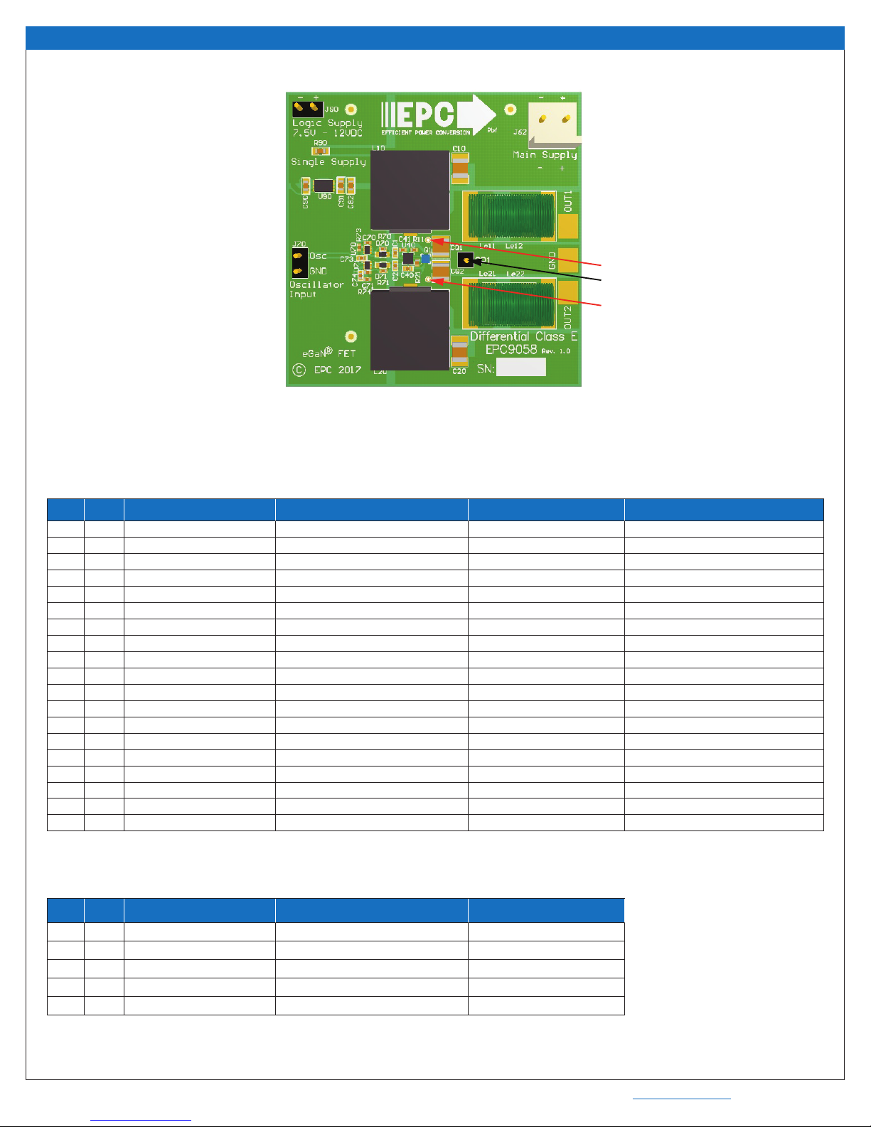
Demonstration System EPC9058
Given these two extremes of the operating load resistance (RLoad), the
optimal point between them must be determined. In this case, the
optimal point yields the same device losses for each of the extreme load
resistance points and is shown in the lower center graph of gure 3. This
optimal design point can be found through trial and error, or using circuit
simulation.
Class-E amplier design
For this amplier only three components need to be specically
designed; 1) the extra inductor (Le), 2) the shunt capacitor (Csh) and, 3) the
selection of a suitable switching device. The RF choke (LRFck) value is less
critical and hence can be chosen or designed.
The design equations for the Class-E amplier have been derived by
N. Sokal [1]. To simplify these equations, the value of QLin [1] is set to
innity, which is a reasonable approximation in most applications within
the frequency capability of this development board. The design needs to
have a specic load resistance (RLoad) value and desired load power (PLoad)
that is used to begin the design, which then drives the values of the other
components, including the magnitude of the supply voltage.
The Class-E amplier passive component design starts with the load
impedancevalue(ZLoad)showningure1.ThereactivecomponentofZLoad
is tuned out using a series capacitor CS, which also serves as a DC block,
resulting in RLoad. It is a common mistake to ignore the need for the DC
block, where a failure to do so can yield a DC current from the supply
through to the load, and lead to additional losses in several components
in that path.
First, using the equations in gure 4, both the extra inductor
Le (equation 2 and shunt capacitor (equation 3) values can be
determined [2], [3]. The value of the shunt capacitor includes the
COSS of the switching device, which must be subtracted from the
calculated value to yield the actual external capacitor (Csh) value. To
do this, rst the magnitude of the supply voltage (VDD) is calculated
using equation 1, which in turn can be used to determine the peak
device voltage (3.56 · VDD).
The RMS value of the peak device voltage is then used to determine the
COSSQ of the device at that voltage. This is the capacitance that will be
deducted from the calculated shunt capacitor to reveal the external
shunt capacitor (Csh) value. The COSSQ of the device can be calculated by
integrating the COSS as function of voltage using equation 4. If the
COSSQ value is larger than the calculated shunt capacitance, the design
cannot be realized for the load resistance specied and a new load
resistance (RLoad) must be chosen.
Finally, the choke (LRFck) can be designed using equation 5 and, in this case,
a minimum value is specied. Larger values yield lower ripple current,
which can lead to a more stable operating amplier. A too-low value will
leadtoincreasedoperatinglossesandchangethemodeofoperationofthe
amplier. In some cases this can be intentional.
Here:
RLoad = Load Resistance [Ω]
PLoad = Load Power [W]
VDD = Amplier Supply Voltage [V]
f = Operating Frequency [Hz]
Le= Extra Inductor [H]
Csh = Shunt Capacitor [F]
COSS = Output Capacitance of the FET [F]
COSSQ = Charge Equivalent Device Output Capacitance [F]
(See gure 6 of the EPC2110 datasheet)
VDS = Drain-Source Voltage of the FET [V]
LRFck = RF Choke Inductor [H]
CS= Series Tuning Capacitor [F]
ZLoad = Load Impedance [Ω]
NOTE.For dierential mode amplier design details, please refer to the
application note ‘AN021: eGaN FETs for Low Cost Resonant Wireless
Power Applications’
[1] N.O. Sokal,“Class-E RF Power Ampliers,”QEX, Issue 204, pp. 9–20,
January/ February 2001.
[2] M. Kazimierczuk, “Collector amplitude modulation of the Class-E
tuned power amplier,”IEEE Transactions on Circuits and Systems,
June 1984, Vol.31, No. 6, pp. 543–549.
[3] Z. Xu, H. Lv, Y. Zhang, Y. Zhang,“Analysis and Design of Class-E Power
Amplier employing SiC MESFETs,“ IEEE International Conference on
Electron Devices and Solid-State Circuits (EDSSC) 2009, 25–27
December 2009, pp 28–31.
QUICK START PROCEDURE
The EPC9058 amplier board is easy to set up to evaluate the
performance of the eGaN FET in a class-E amplier application. Once
the design of the passive components has been completed and
installed, then the board can be powered up and tested.
1. Make sure the entire system is fully assembled prior to making
electrical connections including an applicable load.
2. With power o, connect the main input power supply bus to J62
as shown in gure 5. Note the polarity of the supply connector.
Set the voltage to 0 V.
3. With power o, connect the logic input power supply bus to J90
as shown in gure 5. Note the polarity of the supply connector.
Set the voltage to between 7 V and 12 V.
4. Make sure all instrumentation is connected to the system.
This includes the external oscillator to control the circuit.
5. Turn on the logic supply voltage.
6. Turn on the main supply voltage starting from 0 V, and increase
to the desired value. Note operating conditions and in particular
the thermal performance and voltage of the FETs to prevent over-
temperature and over-voltage failure.
7. Once operation has been conrmed, observe the device voltage,
eciency and other parameters on both the amplier and
device boards.
8. For shutdown, please follow steps in the reverse order.