CMOSTEK CMT2300A Manual de usuario

AN199
Rev 0.8 | Page 1/8
www.cmostek.com
概要
This document discusses the RF frequency calculation formula for CMT2300A / CMT2119B / CMT2219B, which
helps on user design and applications.
The product models covered in this document are shown in the below table.
Table 1. Product Models Covered in This Document
产品型号
工作频率
调制方式
主要功能
配置方式
封装
CMT2300A
126.33 - 1020 MHz
(G)FSK/OOK
Transceiver
Register
QFN16
CMT2119B
126.33 - 1020 MHz
(G)FSK/OOK
Transmitter
Register
QFN16
CMT2219B
126.33 - 1020 MHz
(G)FSK/OOK
Receiver
Register
QFN16
Before reading this document, it is recommended to read the AN142-CMT2300A Quick Start Guide and
AN184-CMT2119B Quick Start Guide to understand the basic information of the 3 products.
目录
1. 射频频率计算 ...............................................................................................................错误!未定义书签。
1.1 配置 RX 的射频参数 .............................................................................................错误!未定义书签。
1.2 配置 TX 的射频参数............................................................................................................................ 5
2. 文档变更记录 ............................................................................................................................................. 7
3. 联系方式..................................................................................................................................................... 8
AN199
CMT2300A / CMT2119B / CMT2219B 射频频率计算指南
Copyright © By CMOSTEK

AN199
Rev 0.8 | Page 2/8
www.cmostek.com
1. RF frequency calculation
The RF frequency calculation and manual configuration methods for the 3 products are described below.
Note that the description of the RX part is not applicable for the CMT2119B and the statement of the TX part is
not applicable for the CMT2219B.
通常情况下,我们建议用户直接使用 RFPDK 来生成参数,并将参数写入频率区的寄存器来完成对射频频
率的配置。如果用户希望在应用程序中单独配置 TX 和RX 的频率,而又不希望使用快速跳频的机制,那么就需
要了解具体配置哪些寄存器,以及这些寄存器的值是如何计算的。下面是频率区的寄存器列表:
In general, when doing the configuration of RF frequency, it's recommend for users to generate
parameters directly using RFPDK and write them to the registers in the frequency area. If users need to
configure the frequency of TX and RX separately in applications without using the fast frequency hopping
mechanism, then it's required to know the detail information of the register configuration and related value
calculation. The registers in the frequency area are listed in the below table.
Table 2. Registers in the Frequency Area
表2. 频率区的寄存器
In the table, the value of FSK_SWT is generated by RFPDK, irrelevant to frequency. Users do not need to
change its value when configuring other bits of the register.
1.1 Configuring RF Parameters of RX
To configure the frequency of the RX, the below items need to be configured.
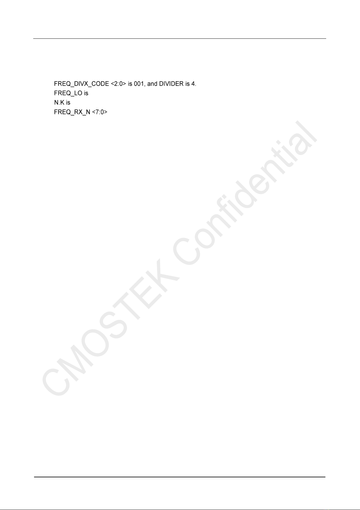
FREQ_VCO_BANK <2:0>
FREQ_DIVX_CODE <2:0>
FREQ_RX_N <7:0>
FREQ_RX_K <19:0>
AFC_OVF_TH <7:0>
其中 N值是频率字的整数部分,K值是频率字的小数部分,DIVX CODE 用于选择 PLL 的分频系数,VCO
BANK 用于选择 VCO 的工作频率区域。计算方式如下:
Among them, N is the integer part of the frequency word, K is the fractional part of the frequency word,
DIVX CODE is used to select the division factor of the PLL, and VCO BANK is used to select the operating
Addr R/W Name Bit 7 Bit 6 Bit 5 Bit 4 Bit 3 Bit 2 Bit 1 Bit 0 Function
0x18 RW CUS_RF1
0x19 RW CUS_RF2
0x1A RW CUS_RF3
0x1B RW CUS_RF4 FREQ_PALDO_SEL
0x1C RW CUS_RF5
0x1D RW CUS_RF6
0x1E RW CUS_RF7
0x1F RW CUS_RF8 FSK_SWT
频率区
FREQ_TX_N [7:0]
FREQ_TX_K [7:0]
FREQ_TX_K [15:8]
FREQ_VCO_BANK [2:0] (000)
FREQ_TX_K [19:16]
FREQ_RX_N [7:0]
FREQ_RX_K [7:0]
FREQ_RX_K [15:8]
FREQ_DIVX_CODE [2:0]
FREQ_RX_K [19:16]

AN199
Rev 0.8 | Page 3/8
www.cmostek.com
frequency range of the VCO. The calculation is as follows.
首先根据希望配置的 RX 频率所属的目标频段,查表得到 FREQ_VCO_BANK<2:0>和
FREQ_DIVX_CODE<2:0>的值(两者都需要写入寄存器),和 分频系数 DIVIDER 的值(用于后续计算 N.K值):
First, check the table to get the value of FREQ_VCO_BANK<2:0> and FREQ_DIVX_CODE<2:0> (both
need to be written to the registers) and DIVIDER (frequency dividing factor, used to calculate N and K)
according to the target frequency band in which the configured frequency is located.
Table 3. Correspondence between PLL analysis parameters and target frequencies.
Target Frequency Band
FREQ_DIVX_CODE <2:0>
DIVIDER
FREQ_VCO_BANK<2:0> = 110
FREQ_VCO_BANK<2:0> = 001
758 840 MHz
840 1020 MHz
000
2
379 420 MHz
420 510 MHz
001
4
189.5 210 MHz
210 255 MHz
010
8
126.33 140 MHz
140 170 MHz
011
12
252.67 280 MHz
280 340 MHz
101
6
然后计算出 LO(本振)的频率。在下面的公式中,FREQ_RF 是目标射频频率,单位是 MHz。FREQ_LO
是计算出的本振频率,单位是 Hz。
Then calculate the frequency of the LO (local oscillator). In the formula below, FREQ_RF is the target RF
frequency in MHz. FREQ_LO is the calculated local oscillator frequency in Hz.
FREQ_LO = FREQ_RF x 10^6 + 26 MHz/92
Then calculate the value of the frequency word N.K.
N.K = FREQ_LO x DIVIDER / 26 MHz
Obtain the integer part of N.K and convert it to binary, which is the value of FREQ_RX_N <7:0>. The fractional
part is multiplied by 2^20 and rounded off, which is the value of the register FREQ_RX_K <19:0>.
The last step is to get the value ofAFC_OVF_TH <7:0>. This register is not in the frequency area. As which is
an important parameter of the receiver AFC algorithm, it is calculated based on the parameters of receivers
such as RX RF frequency, data rate, deviation, and crystal PPM. RFPDK will complete this calculation and
display it on the UI screen as follows.

AN199
Rev 0.8 | Page 4/8
www.cmostek.com
Figure 1. AFC_OVF_TH Screen of RFPDK
User needs to fill in the RF frequency of the RX desired for manual configure in RFPDK, then get the
value of AFC_OVF_TH <7:0>. As the last step, fill it into the register with the address 0x27 CUS_FSK4, to
make the receiver works normally, otherwise the receiver may have error when doing AFC, which may cause
receiving failure.
For example, if the target RF frequency for RX to be configured is 433.92 MHz, according to the above
calculation, it can obtain the followings.
.
.
K is 66.80040135.
is 66 and the corresponding binary is 01000010.
FREQ_RX_K <19:0> is 839282 and the corresponding.
in RFPDK.
To configure the TX frequency, you need to configure:

AN199
Rev 0.8 | Page 5/8
www.cmostek.com
1.2 配置 TX 的射频参数 Configure RF Parameters for TX
Followings need to be configured for TX.
FREQ_VCO_BANK <2:0>
FREQ_DIVX_CODE <2:0>
FREQ_TX_N <7:0>
FREQ_TX_K <19:0>
FREQ_PALDO_SEL
Among them, FREQ_VCO_BANK<2:0> and FREQ_DIVX_CODE <2:0> are obtained in the same way as in
RX, that is, TX and RX share DIVX CODE and VCO BANK. If the target frequency bands are not the same,
when each time TX or RX is configured, recalculation and writing to these two registers is needed.
Then calculate the frequency of the LO (local oscillator), which is different from the LO frequency of RX. In the
formula below, FREQ_RF is the target RF frequency in MHz. FREQ_LO is the calculated local oscillator
frequency in Hz.
FREQ_LO = FREQ_RF x 10^6
Then calculate the value of the frequency word N.K, which is the same as the R.N.K value calculation
formula:
N.K = FREQ_LO x DIVIDER / 26MHz
At last, check the table below to get the value of FREQ_PALDO_SEL:
TX
Frequency
FREQ_PALDO_SEL
< 500 MHz
0
>= 500 MHz
1
举个例子,如果需要配置的 TX 目标射频频率是 433.92 MHz,根据上面的计算步骤,得出:
TX frequency FREQ_PALDO_SEL
< 500 MHz 0
>= 500 MHz 1
For example, if the target RF frequency for TX to be configured is 433.92 MHz, according to the above

AN199
Rev 0.8 | Page 6/8
www.cmostek.com
calculation, it can obtain the followings.
FREQ_VCO_BANK <2:0> is 001.
433920000.
66.75692308.
is 66 and the corresponding binary is 01000010
FREQ_RX_K <19:0> is 793691 and the corresponding is 11000001110001.
FREQ_PALDO_SEL is 0..
FREQ_VCO_BANK <2:0>的值是 001
FREQ_DIVX_CODE <2:0>是001,DIVIDER 的值是 4
FREQ_LO 的值是 433920000
N.K 的值是 66.75692308
FREQ_RX_N <7:0>的值是 66,二进制是 01000010
FREQ_RX_K <19:0>的值是 793691,二进制是
FREQ_PALDO_SEL 是0

AN199
Rev 0.8 | Page 7/8
www.cmostek.com
2. 文档变更记录
表3. 文档变更记录表
版本号
章节
变更描述
日期
0.8
所有
初始版本发布
2017-10-31

AN199
Rev 0.8 | Page 8/8
www.cmostek.com
3. 联系方式
无锡泽太微电子有限公司深圳分公司
中国广东省深圳市南山区前海路鸿海大厦 203 室
邮编: 518000
电话: +86 - 755 - 83235017
传真: +86 - 755 - 82761326
销售: sales@cmostek.com
技术支持: support@cmostek.com
网址: www.cmostek.com
The information furnished by CMOSTEK is believed to be accurate and reliable. However, no responsibility is assumed for
inaccuracies and specifications within this document are subject to change without notice. The material contained herein is
the exclusive property of CMOSTEK and shall not be distributed, reproduced, or disclosed in whole or in part without prior
written permission of CMOSTEK. CMOSTEK products are not authorized for use as critical components in life support
devices or systems without express written approval of CMOSTEK. The CMOSTEK logo is a registered trademark of
CMOSTEK Microelectronics Co., Ltd. All other names are the property of their respective owners.
Copyright. CMOSTEK Microelectronics Co., Ltd. All rights are reserved.
Otros manuales para CMT2300A
3
Este manual sirve para los siguientes modelos
2
Tabla de contenidos
Otros manuales de Transceptor de CMOSTEK

CMOSTEK
CMOSTEK CMT2300A-EQR Manual de usuario

CMOSTEK
CMOSTEK CMT2300A Manual de funcionamiento

CMOSTEK
CMOSTEK CMT2380F64 Manual de usuario

CMOSTEK
CMOSTEK CMT2300A Manual de usuario

CMOSTEK
CMOSTEK CMT2300A Manual de usuario

CMOSTEK
CMOSTEK CMT2310A Manual de usuario

CMOSTEK
CMOSTEK CMT216 Series Manual de usuario

CMOSTEK
CMOSTEK CMT2300AW Manual de instrucciones

CMOSTEK
CMOSTEK CMT2380F17 Manual de usuario


