
Applied Data Systems Bitsy Manual de usuario

Bitsy
User’s Manual
ADS document # 110111-1003A
Applied Data Systems
www.applieddata.net
9140 Guilford Road
Columbia MD 21046
301-490-4007
© 2001 ADS


Bitsy User’s Manual
ADS document # 110111-1003A Page i
Revision History
ADS document # 110111-1003A.
REV DESCRIPTION DATE BY
1 Initial release 06/20/01 HW
A
Correct Header Information
1.2:
Clearify Features
1.3:
Update Block Diagram
J7:Add Illustration for pin locations
J1:Add note
Correct Pin 28 description
J3:Modify Descriptions for Pin 1, 2, 16 and 18
J6:Modify Pin 1 description to 5-12V
Added 4.1.3 Using Compact Flash Interface
Added 4.1.4 Using USB Interface
4.3.1:
Modified Maximum voltage 10 12V
4.3.2:
Modified to maximum 12V
4.3.7:
Added notes
4.4:
Removed VDDI (1.75V) and +30V for J3
and Panel VEE for J1 from table
4.5:
Corrected mA reference for fully populated
board
Removed footnote 1
4.7:
Added Protection
4.8:
Added information to 4.8.1 Analog Inputs
Added SA1111 information
5.1.2:
Corrected Rev B description to 12V
07/03/01 PD
About the Cover Photo
The cover photo shows a fully populated Rev B Bitsy with 16MB of onboard flash.

Bitsy User’s Manual
Page ii ADS document # 110111-1003A
(This page intentionally blank)

Bitsy User’s Manual
ADS document # 110111-1003A Page iii
Table of Contents
Revision History....................................................................................................................................................i
About the Cover Photo..........................................................................................................................................i
Table of Contents ................................................................................................................................................iii
1Introduction...................................................................................................................................... 1
1.1 Overview ................................................................................................................................ 1
1.2 Features................................................................................................................................... 1
1.2.1 Processor ...................................................................................................................... 1
1.2.2 Power Supply................................................................................................................ 1
1.2.3 Memory........................................................................................................................ 1
1.2.4 Communications........................................................................................................... 1
1.2.5 User Interface and Display ........................................................................................... 1
1.2.6 I/O................................................................................................................................. 2
1.2.7 Audio Interface............................................................................................................. 2
1.3 Block Diagram........................................................................................................................ 3
2Getting Started.................................................................................................................................. 5
2.1 Evaluation Systems................................................................................................................. 5
2.2 Frequently Asked Questions................................................................................................... 5
2.3 Organization of this Manual ................................................................................................... 6
2.4 For Further Information.......................................................................................................... 6
3Hardware Reference......................................................................................................................... 7
3.1 Locating "Pin 1" ..................................................................................................................... 7
3.2 Switches.................................................................................................................................. 7
3.2.1 S1: DIP Switch ............................................................................................................ 7
3.3 ADSmartIOTM......................................................................................................................... 7
3.4 Onboard LEDs........................................................................................................................ 7
3.5 Jumper Settings....................................................................................................................... 7
3.5.1 JP1, JP2: VEE Contrast Voltage Control..................................................................... 7
3.5.2 JP3: Flat Panel Voltage Select..................................................................................... 8
3.5.3 JP4: Flat Panel Data Voltage Select ............................................................................ 8
3.5.4 J7: Flat Panel VEE Select............................................................................................ 8
3.6 Connector Pinouts................................................................................................................... 8
3.6.1 J1: LCD Panel Interface Connector............................................................................. 9

Bitsy User’s Manual
Page iv ADS document # 110111-1003A
3.6.2 J2: PCMCIA.............................................................................................................. 10
3.6.3 J3: High Density IO connector.................................................................................. 10
3.6.4 J4: Manufacturing Test Connector: ........................................................................... 11
3.6.5 J5: Manufacturing JTAG Test Connector:................................................................. 11
3.6.6 J6: Line Input Power Connector:............................................................................... 11
3.6.7 J8: Touch Screen Connector:..................................................................................... 11
3.6.8 J9: High Density External Compact Flash Signal Connector:................................... 12
3.6.9 J10: High Density IO connector:............................................................................... 13
3.6.10 Functions of SA1110 GPIOs:................................................................................... 14
4System Integration.......................................................................................................................... 15
4.1 Tips for System Integration .................................................................................................. 15
4.1.1 Strategies for Backup Power ...................................................................................... 15
4.1.2 Electrical Tips............................................................................................................. 15
4.1.3 Utilizing the Compact Flash Interface........................................................................ 15
4.1.4 Using the USB Interface............................................................................................. 15
4.1.5 Bitsy Power Supply.................................................................................................... 15
4.2 Mechanical Specifications.................................................................................................... 16
4.2.1 Mechanical Drawing................................................................................................... 16
4.2.2 Mounting Holes.......................................................................................................... 16
4.2.3 Clearances .................................................................................................................. 17
4.3 Input Power Requirements.................................................................................................... 17
4.3.1 DC power input .......................................................................................................... 17
4.3.2 Main battery input ...................................................................................................... 17
4.3.3 3V Backup battery input............................................................................................. 17
4.3.4 Switching Supply Outputs.......................................................................................... 17
4.3.5 Backlight Power ......................................................................................................... 17
4.3.6 EMI/RFI and Transient Suppression.......................................................................... 18
4.4 Externally Available Voltages.............................................................................................. 18
4.5 Power Consumption.............................................................................................................. 18
4.6 Power Management.............................................................................................................. 18
4.7 EMI/RFI and ESD Protection............................................................................................... 19
4.8 Electrical Specifications for I/O Ports .................................................................................. 19
4.8.1 ADSmartIOTM Controller ........................................................................................... 19
4.8.2 UCB 1200................................................................................................................... 19
4.8.3 LCD Panel.................................................................................................................. 20
4.8.4 SA1111....................................................................................................................... 20
4.8.5 SA-1110...................................................................................................................... 20
5Board Revision History..................................................................................................................21
5.1.1 Identifying the board revision..................................................................................... 21
5.1.2 Revision History......................................................................................................... 21

Bitsy User’s Manual
ADS document # 110111-1003A Page 1
1 Introduction
1.1 Overview
The Bitsy is a full-featured single board computer using the SA-1110 StrongARM RISC
microprocessor. The Bitsy is designed to meet the needs of embedded and graphical systems
developers.
1.2 Features
1.2.1 Processor
• SA-1110 32-bit StrongARM
• SA-1111 Companion Chip
• Clock rates up to 206 MHz
1.2.2 Power Supply
• 5-12V Input Range
• DC/Battery Switching
• Battery Charger
1.2.3 Memory • 16, 32 or 64 MB synchronous DRAM (Runs 1/2 of CPU clock rate)
• 8, 16 or 32 MB Flash
• 3.3 and 5V PCMCIA
1.2.4 Communications
• Ethernet, RJ45 (with optional connector board)
• CompactFlash interface (with optional connector board)
• USB Master and Slave connections, Support for 12Mb/s
• Three Serial Ports
Serial 1: RS-232, TTL
Serial 2: TTL, RS-232 (IrDA with optional connector board)
Serial 3: RS-232, TTL
1.2.5 User Interface and Display
• Flat panel interface
• Onboard VEE generator with software contrast control
• Analog touch panel interface

Bitsy User’s Manual
Page 2 ADS document # 110111-1003A
1.2.6 I/O • ADSmartIOTM configurable for digital I/O, PWM and A/D inputs
• Up to eight analog inputs
• Up to 25 Digital I/O
• Backlight control signals for intensity and on/off
• Passive LCD contrast control
• External temperature probe support
1.2.7 Audio Interface
• Input mono microphone to UCB1200 codec
• Output mono speaker from UCB1200 codec
• Input stereo microphone to UDA1341 stereo codec
• Output stereo speaker from UDA1341 stereo codec
Bitsy User’s Manual
ADS document # 110111-1003A Page 3
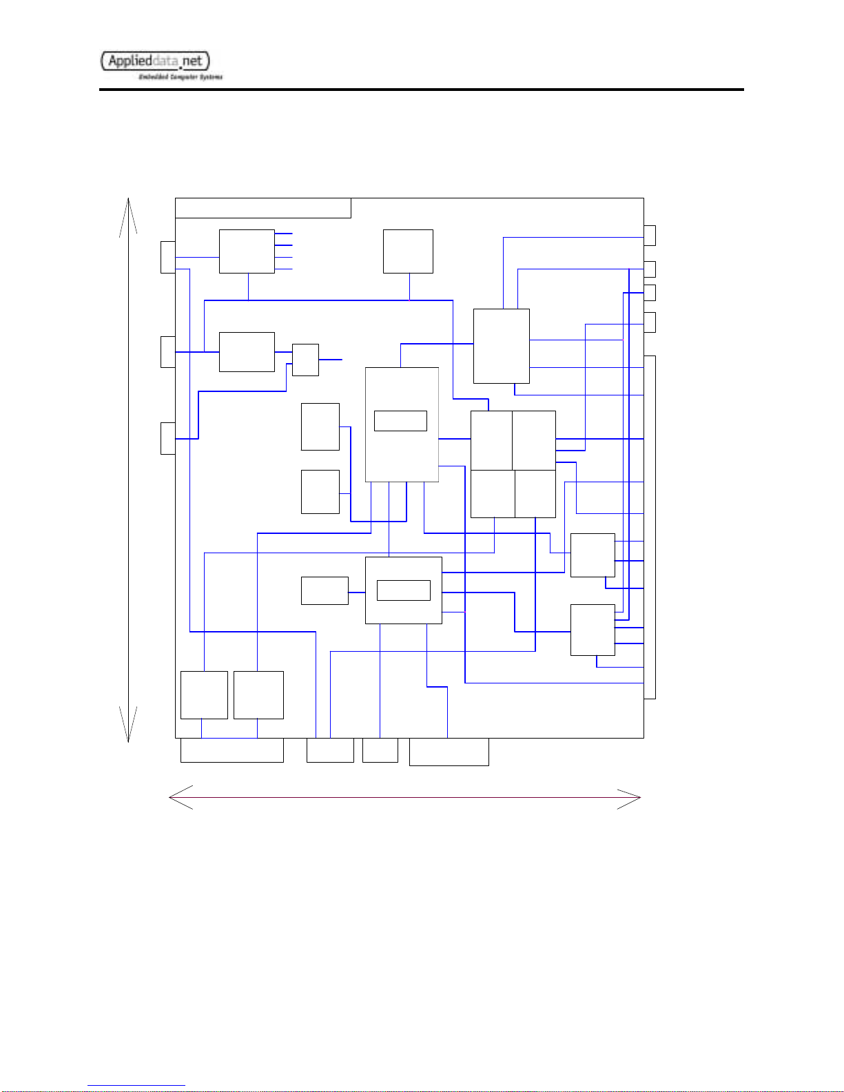
1.3 Block Diagram
The following diagram illustrates the system organization of the Bitsy.
Compact
FLASH
Interface
Software
Switches
(2)
PS2 Keyboard
5V/3V Panel
Audio
Codec
UDA1341
Switch
FLASH
8/16/32
Mbytes
COMPACT
FLASH/EXPANSION
CONNECTOR
Keypad
Scanner
Back Light
PCMCIA
SDRAM
16/32/64
Mbytes
BITSY
Line Inputs L/R
Battery Power
Input DC Power Input
SERIAL
BATTERY
CHARGER
Speaker 1
COM2
3V CMOS/IRDA
SA1110
USB Slave/
USB Master
Microphone 2
CODEC
UCB1200
5V
COM3
4 WIRE RS232
10 Digital IOs
High Density I/O Connectors
ADS Smart
Configurable
IOs
Speaker 2
3"
VEE
Generator
RS232
Drivers
Power
Supply
Power
Management
SSP
Microphone 1
4 Analog
Inputs
30V
COM1
8 WIRE
RS232
12V BL
+3.3V
4 Wire Analog
Touch Screen
Regulator
SA1111
PWM1
Smart
Configurable
IOs
5-12VDC
+1.75V
5"
Backup
Battery
PWM2
+3.3VCONT
Panel Driver

Bitsy User’s Manual
Page 4 ADS document # 110111-1003A
(This page intentionally blank)
Tabla de contenidos
Otros manuales de Placa madre de Applied Data Systems

Manuales populares de Placa madre de otras marcas


Telit Wireless Solutions
Telit Wireless Solutions SL869-3DR Manual de usuario

Gigabyte
Gigabyte GA-9IVDT Manual de usuario

Texas Instruments
Texas Instruments ADS8372EVM Manual de usuario

Commell
Commell MS-C73 Manual de usuario

IBT Technologies
IBT Technologies MB860 Manual de usuario

Nvidia
Nvidia TEGRA DG-04927-001_V01 Manual de usuario


